Texturing and cleaning process method of polysilicon wafer

A technology for polycrystalline silicon wafers and silicon wafers, applied in cleaning methods and utensils, cleaning methods using liquids, chemical instruments and methods, etc., can solve the problems of difficult control of product quality, increase production costs, etc., and achieve remarkable results and improve the effect. , the effect of low investment cost

Active Publication Date: 2013-06-12
CHANGZHOU S C EXACT EQUIP
View PDF4 Cites 45 Cited by
  • Summary
  • Abstract
  • Description
  • Claims
  • Application Information

AI Technical Summary

Problems solved by technology

In the above-mentioned traditional process method, to improve the conversion efficiency of the battery sheet by 0.2-0.3%, SE (selective emitter cell technology), back polishing (the back of the diffused silicon wafer is chemically polished to increase the reflectivity to 30%) Above), DP (printing the gate lines of the silicon wafer twice), back passivation (plating a passivation layer on the back of the silicon wafer) and other high-cost complex processes increase the manufacturing cost, and the product quality is difficult to control

Method used


Image

  • Texturing and cleaning process method of polysilicon wafer

Examples


Embodiment Construction

[0018] The invention will be described in detail below with reference to the accompanying drawings and embodiments.

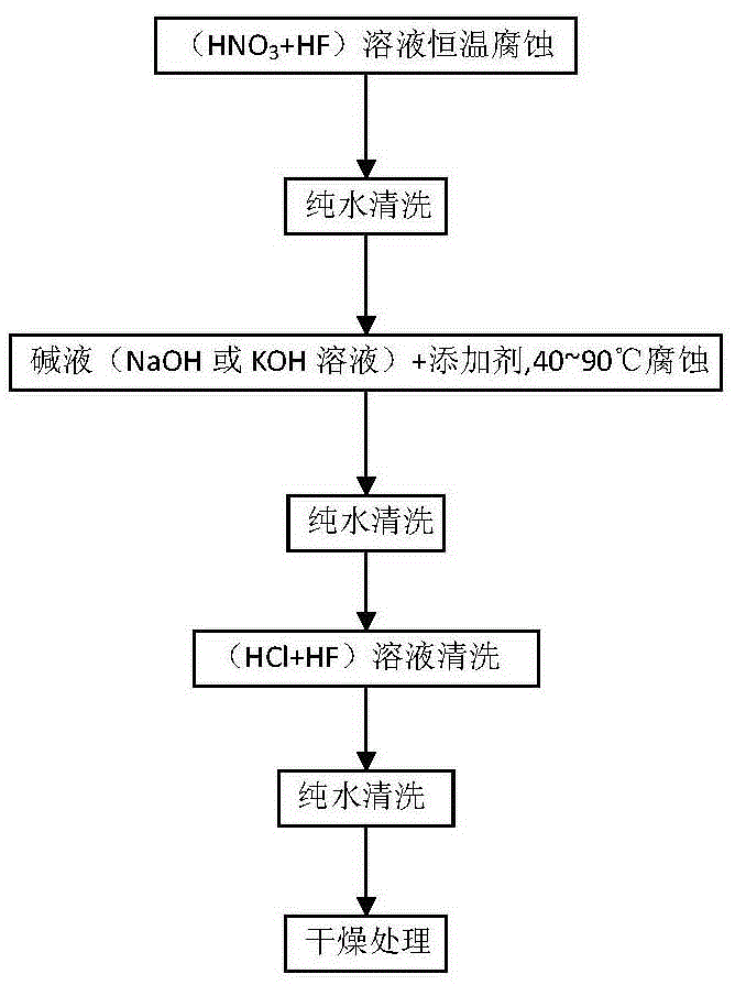
[0019] like figure 1 As shown, the texturing and cleaning process of the polycrystalline silicon wafer proposed by the present invention includes the following steps:

[0020] 1. The silicon wafer is first soaked in a mixed solution of 5-7.5% HF and 35-45% HNO3 with a temperature control of 5-15°C for 0.8-1.5 minutes, and then acid etching is performed to achieve the purpose of preliminary texturing of the silicon wafer. . In this process, according to the consumption of the reaction between the solution and the silicon wafer, a certain amount of HF and HNO3 are replenished in time to ensure the proper ratio of the solution;

[0021] 2. The silicon wafer after acid etching is then cleaned in 10-18MΩ·cm pure water by spraying, soaking or a combination of the two methods, in order to minimize the adhesion of the acid solution on the surface of the silicon wafer...


PUM


Abstract

The invention discloses a texturing and cleaning process method of a polysilicon wafer. The method comprises the following steps of 1, firstly, putting the polysilicon wafer in a mixing solution of HF (hydrogen fluoride) and HNO3 (hydrogen nitrate), and soaking; 2, putting the polysilicon wafer corroded by acid into pure water, and cleaning; 3, putting the polysilicon wafer in an alkaline solution, carrying out alkaline corrosion treatment, adding a texturing additive into the alkaline solution, and carrying out secondary texturing on the polysilicon wafer; 4, putting the polysilicon wafer corroded by alkali into the pure water, and cleaning; 5, putting the polysilicon wafer in a mixing solution of HCl (hydrogen chloride) and HF, and soaking; 6, putting the polysilicon wafer corroded by the acid into the pure water, and cleaning; and 7, drying the treated polysilicon wafer. The process method has the advantages that on the premise of not changing other processes, the final converting efficiency of the polysilicon wafer is improved by 0.2% to 0.3%, and the purpose of final efficiency stacking of a battery sheet is realized.

Description

technical field [0001] The invention relates to the field of solar silicon wafer cleaning and drying equipment, in particular to a texturing cleaning process for polycrystalline silicon wafers applied in the photovoltaic industry. Background technique [0002] In the production of polycrystalline silicon wafers, texturing and cleaning are required. The traditional process includes low temperature and high concentration acid texturing, normal temperature low concentration acid texturing, dilute alkali washing, deionization and passivation. In the above traditional process method, to improve the conversion efficiency of the cell by 0.2-0.3%, SE (selective emitter cell technology), back polishing (the back of the diffused silicon wafer is chemically polished to increase the reflectivity to 30%) High-cost and complex processes such as the above), DP (printing the gate lines of the silicon wafer twice), and back passivation (coating a passivation layer on the back of the silicon...

Claims


Application Information

Patent Timeline
Patent Type & Authority Applications(China)
IPC IPC(8): H01L31/18C30B33/10B08B3/08B08B3/02B08B3/04
CPCY02P70/50
Inventor 左国军李国庆
Owner CHANGZHOU S C EXACT EQUIP
Why Eureka
Try Eureka