Check patentability & draft patents in minutes with Patsnap Eureka AI!

Low thermal resistance led packaging structure and packaging method

A technology of LED encapsulation and encapsulation method, which is applied in the direction of electrical components, electric solid devices, circuits, etc. It can solve the problems of difficult circuit processing on the surface, difficulty in realization, and large radiator volume, so as to improve light extraction efficiency and product consistency. , Brightness and Reliability Improvement Effect

Active Publication Date: 2017-02-08
INST OF SEMICONDUCTORS - CHINESE ACAD OF SCI
View PDF5 Cites 0 Cited by
  • Summary
  • Abstract
  • Description
  • Claims
  • Application Information

AI Technical Summary

Problems solved by technology

[0004] The best way is to directly solder the LED chip to the heat sink through solder. The heat generated by the LED chip can reach the final heat sink only through a layer of dielectric layer (solder) from the LED chip itself, so that the series thermal resistance is the smallest. However, the radiator has a large volume and the surface is not easy to process the circuit, making this method very difficult to realize.

Method used


Image

  • Low thermal resistance led packaging structure and packaging method
  • Low thermal resistance led packaging structure and packaging method
  • Low thermal resistance led packaging structure and packaging method

Examples


Embodiment Construction

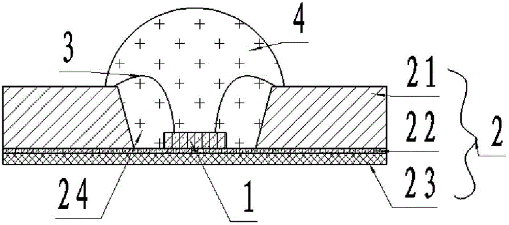
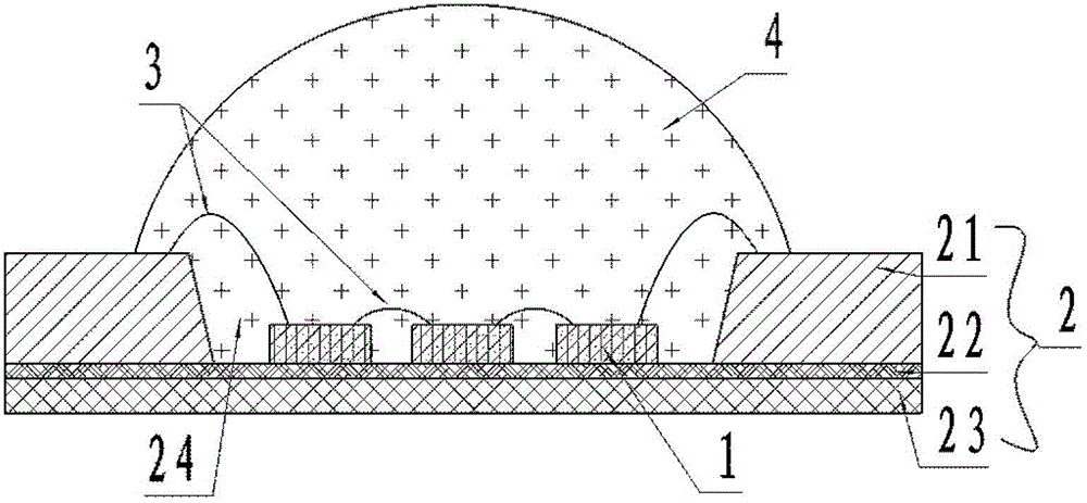
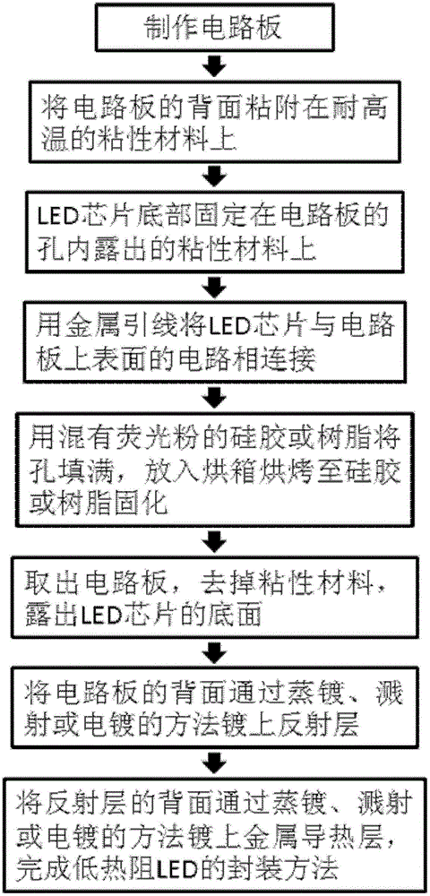
[0023] see figure 1 and figure 2 As shown, the present invention provides a low thermal resistance LED packaging structure, which includes:

[0024] LED chip 1, the number of the LED chip 1 is greater than or equal to 1, figure 1 The number of LED chip 1 is one, figure 2 The number of LED chips 1 is multiple, the LED chip 1 is a solid semiconductor chip, and its luminescent material is a luminescent material of red light, blue light, green light or ultraviolet light, and the LED chip 1 can be a high-power chip, a medium-power chip, Or a low-power chip, the LED chip 1 can be one LED chip, can also be composed of multiple single-wavelength LED chips connected in series and parallel, or can be composed of multiple multi-wavelength LED chips connected in series and parallel. The LED chip 1 is a single-wavelength or multi-wavelength LED chip. When there are multiple LED chips 1, the LED chips 1 are connected in series or in parallel (see figure 2 );

[0025] A supporting ci...


PUM


Abstract

A low thermal resistance LED packaging structure, which includes: LED chips; a supporting circuit board, including: a circuit board; a reflective layer made under the circuit board and a metal heat conducting layer made under the reflective layer, the circuit board There is a through hole in the middle, and the LED chip is located in the through hole of the circuit board, and the LED chip is electrically connected to the circuit board through a metal lead; the sealing layer seals the electrically connected LED chip on the Inside the through hole of the circuit board in the support circuit board. The advantage of the present invention is that there is no support, the LED packaging structure can improve the light output efficiency of the LED chip, and the heat generated by the LED chip can be rapidly diffused through the metal heat conducting layer, and then transferred to the surface of the radiator, saving the intermediate link of the traditional packaging structure, The thermal resistance is significantly reduced, the brightness and reliability are improved, the overall production cost is reduced, and the product consistency is improved.

Description

technical field [0001] The invention belongs to the technical field of semiconductors, in particular to a packaging structure and packaging method of a light-emitting diode (LED) with low thermal resistance. Background technique [0002] As a new type of high-efficiency solid light source, light-emitting diode (LED) has significant advantages such as long life, energy saving, and environmental protection. It is another leap in the history of human lighting after incandescent lamps and fluorescent lamps. New technology has huge economic and social significance. [0003] With the continuous development of semiconductor technology, LED technology has developed rapidly, and the performance of LED parameters such as luminous intensity, peak wavelength, and half-wave bandwidth has been greatly improved. Like traditional light sources, semiconductor light-emitting diodes (LEDs) also generate heat during operation, the amount of which depends on the overall luminous efficiency. Un...

Claims


Application Information

Patent Timeline
Patent Type & Authority Patents(China)
IPC IPC(8): H01L33/48H01L33/54H01L33/64
CPCH01L2224/48091H01L2224/48137H01L2924/00014
Inventor 卢鹏志杨华郑怀文于飞薛斌伊晓燕王国宏王军喜李晋闽
Owner INST OF SEMICONDUCTORS - CHINESE ACAD OF SCI
Features
  • R&D
  • Intellectual Property
  • Life Sciences
  • Materials
  • Tech Scout
  • Unparalleled Data Quality
  • Higher Quality Content
  • 60% Fewer Hallucinations
Learn More