Photovoltaic device and manufacturing method thereof

A photovoltaic device and substrate technology, applied in photovoltaic power generation, semiconductor devices, electrical components, etc., can solve the problem of low recombination speed, achieve low recombination speed, prevent open circuit voltage (Voc, high back reflectivity effect)

Inactive Publication Date: 2016-10-26
MITSUBISHI ELECTRIC CORP
View PDF12 Cites 0 Cited by
  • Summary
  • Abstract
  • Description
  • Claims
  • Application Information

AI Technical Summary

Problems solved by technology

In this case, there is a problem that especially during firing, the contaminants will adhere to and fix on the back surface of the substrate, so there is a need to suppress the recombination speed of the carrier on the back surface of the substrate to a relatively low speed. low is extremely difficult

Method used


Image

  • Photovoltaic device and manufacturing method thereof
  • Photovoltaic device and manufacturing method thereof
  • Photovoltaic device and manufacturing method thereof

Examples


Embodiment approach 1

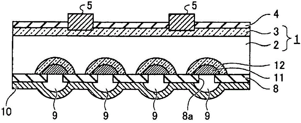
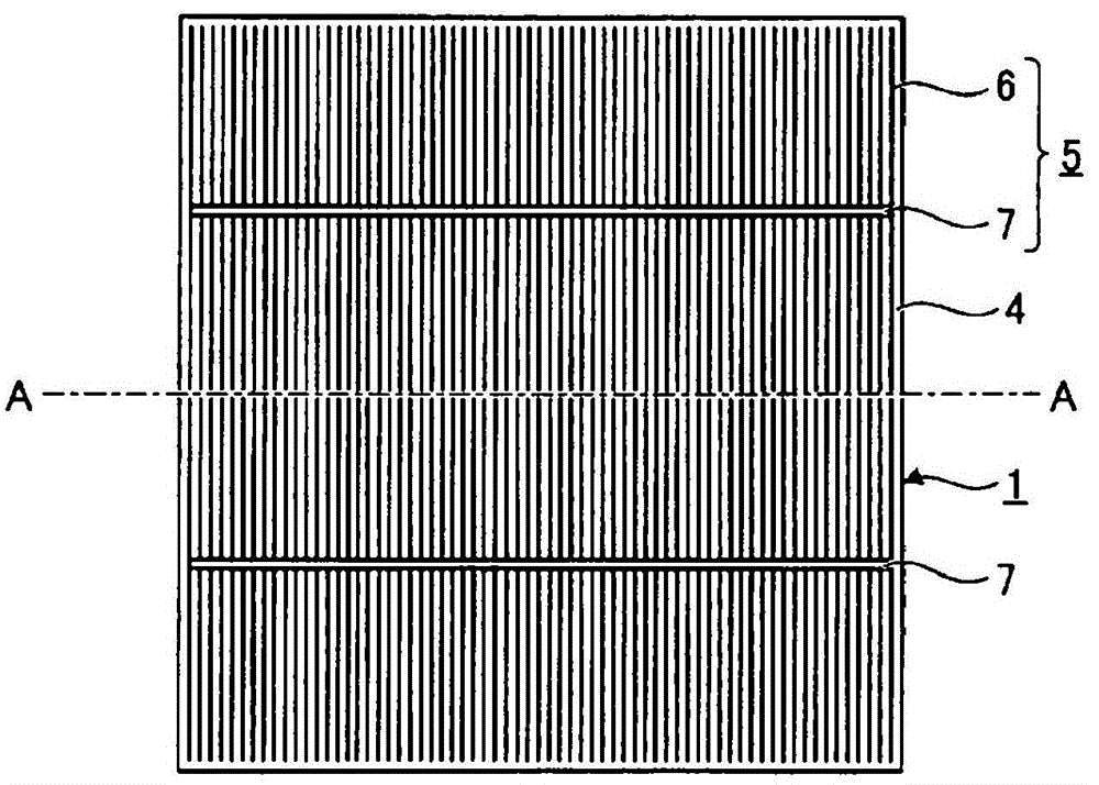
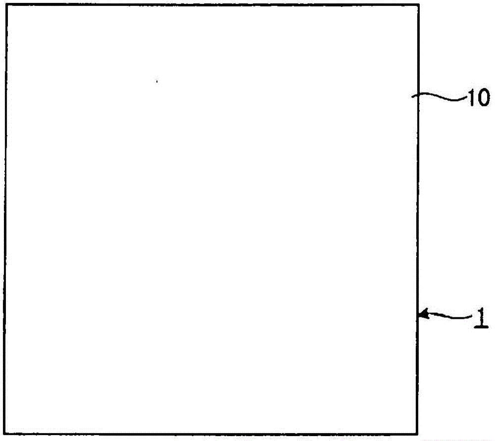
[0044] FIGS. 1-1 to 1-3 are diagrams showing the structure of a solar battery cell as a photovoltaic device according to this embodiment, and FIG. 1-1 is a sectional view of main parts for explaining the cross-sectional structure of a solar battery cell, and FIG. 1-2 It is a plan view of the solar battery cell viewed from the light-receiving surface side, and Fig. 1-3 is a bottom view of the solar battery cell viewed from the side opposite to the light-receiving surface (rear side). Fig. 1-1 is a sectional view of main parts taken along line A-A of Fig. 1-2.

[0045]The solar cell unit of this embodiment is shown in Figures 1-1 to 1-3, including: a semiconductor substrate 1, which has a pn junction (p-n junction), and is a solar cell substrate with a photoelectric conversion function; an anti-reflection film 4. It is formed on the light-receiving surface side (front surface) of the semiconductor substrate 1, and is an insulating film that prevents reflection of incident light ...

Embodiment approach 2

[0103] In Embodiment 2, as another form of the back reflection film 10 , a case where the back reflection film 10 is made of a metal foil will be described. Figure 7 It is a sectional view of main parts for explaining the sectional structure of the solar battery cell of this embodiment, and is a figure corresponding to FIG. 1-1. The difference between the solar battery cell of Embodiment 2 and the solar battery cell of Embodiment 1 is that the back reflective film is not a silver sputtered film but is made of aluminum foil. The configuration other than this is the same as that of the solar battery cell according to Embodiment 1, so detailed description thereof will be omitted.

[0104] Such as Figure 7 As shown, in the solar battery cell of this embodiment, on the back surface of the semiconductor substrate 1, the conductive adhesive 21 arranged on the back aluminum electrode 9 covers the back aluminum electrode 9 and the back insulating film 8. A rear reflective film 22 m...

Embodiment approach 3

[0117] In Embodiment 3, an embodiment in which degradation of characteristics due to burn-through is prevented in the solar cells of Embodiments 1 and 2 described above will be described.

[0118] In terms of increasing the efficiency of crystalline silicon solar cells, the suppression of the recombination rate on the rear surface has recently become more and more important. Instances where the diffusion length of the carrier is greater than the thickness of the silicon substrate are by no means uncommon in both monocrystalline silicon solar cells and polycrystalline silicon solar cells. Therefore, the magnitude of the surface recombination velocity on the back surface of the silicon substrate greatly affects the characteristics of the solar cell.

[0119] On the other hand, when processing from a solar battery cell as a device unit to a solar battery module as an actual product, a plurality of solar battery cells are connected in series or in series or in parallel via metal f...


PUM


Abstract

Including: a semiconductor substrate (substrate), which has an impurity diffusion layer; a first electrode, which penetrates an anti-reflection film formed on the impurity diffusion layer and is electrically connected to the impurity diffusion layer; A plurality of openings on the other side of the bottom; a second electrode formed on the other side of the substrate; a back reflective film made of a metal film formed by a vapor phase growth method or containing metal foil, the back reflector The film is formed to cover at least the back insulating film, and the second electrode includes: an aluminum-based electrode made of a material containing aluminum, embedded in at least the opening on the other side of the substrate, and electrically connected to the other side of the substrate; A silver-based electrode made of a material containing silver is provided in a region between the openings on the other side of the substrate in a state of being inserted into the back insulating film so as to be insulated from the other side of the substrate by the back insulating film, And the silver-based electrode is electrically connected to the aluminum-based electrode via the back reflection film.

Description

technical field [0001] The invention relates to a photovoltaic device and a manufacturing method thereof. Background technique [0002] In recent photovoltaic devices, improvements in raw materials and manufacturing processes are being promoted with the aim of increasing output. Therefore, in order to achieve further higher output, it is important to confine light in the photovoltaic device and suppress the recombination speed of the carriers on the front and back, so that light in a wavelength range that has not been fully utilized before is realized. Structure and manufacturing method to support power generation. Therefore, it is very important to improve the structure of the back surface of the substrate which plays a part of the role. [0003] For this reason, the following technology is advocated: aiming at suppressing the reflection on the back side of the substrate and the recombination speed on the back side of the substrate, for example, suppressing the recombinat...

Claims


Application Information

Patent Timeline
Patent Type & Authority Patents(China)
IPC IPC(8): H01L31/0224H01L31/068H01L31/056
CPCH01L31/022425H01L31/068Y02E10/52Y02E10/547H01L31/056H01L31/02327
Inventor 滨本哲
Owner MITSUBISHI ELECTRIC CORP
Why Eureka
Try Eureka