Adhesive film and electronic device including the same
An adhesive film, semiconductor technology, applied in and used in the semiconductor field, can solve the problems of reduced chip shear strength, difficult to remove pores, and deteriorating workability, to ensure pore characteristics, high reliability, and easy removal. , to ensure the effect of reliability
- Summary
- Abstract
- Description
- Claims
- Application Information
AI Technical Summary
Problems solved by technology
Method used
Image

Examples
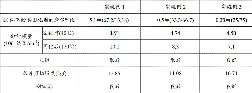
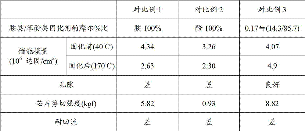
Embodiment 1
[0092] Preparation of adhesive films for semiconductors containing both amine and phenolic curing agents
[0093] Based on the solid content of 100 parts by weight of the adhesive film, 67.7 parts by weight of elastomer resin (AD-102S, Daiichi Textile Industry Co., Ltd.), 13.5 parts by weight of epoxy resin (EPPN-502H, Japan Chemical Co., Ltd. ), 7.8 parts by weight of amine curing agent (DDS, Wako), 1.5 parts by weight of phenolic curing agent (BPA, KukdoChemical Co., Ltd.) (hydroxyl equivalent: 114g / eq), 0.5 parts by weight of silane coupling agent (S -510, Chisso) and 9 parts by weight of filler (R-972, Degussa) were dissolved in cyclohexanone as an organic solvent, fully kneaded with a bead mill and deposited on the release-treated on PET film. The mixture was then dried in an oven at 100° C. for 20 minutes, thereby preparing an adhesive film for semiconductors having a thickness of 60 μm.
Embodiment 2
[0095] Preparation of adhesive films for semiconductors containing both amine and phenolic curing agents
[0096] In addition to the solid content based on 100 parts by weight of the adhesive film, 12.3 parts by weight of epoxy resin (EPPN-502H, Japan Chemical Co., Ltd.), 5.5 parts by weight of amine curing agent (DDS, Wako) and 5.0 parts by weight of The adhesive film for semiconductor was prepared in the same manner as in Example 1 except for the phenolic curing agent (BPA, Kukdo Chemical Co., Ltd.).
Embodiment 3
[0098] Preparation of Adhesive Films for Semiconductors Containing Both Amine Curing Agents and Phenolic Curing Agents
[0099] In addition to the solid content based on 100 parts by weight of the adhesive film, 11.7 parts by weight of epoxy resin (EPPN-502H, Japan Chemical Co., Ltd.), 3.9 parts by weight of amine curing agent (DDS, Wako) and 7.2 parts by weight of The adhesive film for semiconductor was prepared in the same manner as in Example 1 except for the phenolic curing agent (BPA, Kukdo Chemical Co., Ltd.).
PUM
| Property | Measurement | Unit |
|---|---|---|
| epoxy equivalent | aaaaa | aaaaa |
| epoxy equivalent | aaaaa | aaaaa |
| particle size | aaaaa | aaaaa |
Abstract
Description
Claims
Application Information