Thin film transistor (TFT) array substrate and manufacture method and display device thereof

A technology of an array substrate and a manufacturing method, applied in the display field, can solve the problems of large exposure, damage to the active layer, increase in the manufacturing cost of the array substrate, etc., and achieve the effects of reducing costs, ensuring characteristics, and overcoming damage

Inactive Publication Date: 2015-01-28
BOE TECH GRP CO LTD
View PDF5 Cites 0 Cited by
  • Summary
  • Abstract
  • Description
  • Claims
  • Application Information

AI Technical Summary

Problems solved by technology

Therefore, regardless of the above process sequence, exposure must be performed when making the resin flat layer, and the exposure amount is relatively large. Large exposure amount will damage the active layer (including the semiconductor layer and the doped semiconductor layer), which will affect the TFT. feature, reducing display quality
[0004] One of the current solutions is to add a masking process to make the light-shielding pattern on the top of the TFT, but adding a masking process will greatly increase the manufacturing cost of the array substrate. With other patterns (such as: passivation layer via pattern), it will increase the cost of the mask plate and increase the manufacturing cost of the array substrate

Method used


Image

  • Thin film transistor (TFT) array substrate and manufacture method and display device thereof
  • Thin film transistor (TFT) array substrate and manufacture method and display device thereof
  • Thin film transistor (TFT) array substrate and manufacture method and display device thereof

Examples


Embodiment 1

[0038] combine Figure 1-Figure 8 As shown, the manufacturing method of the TFT array substrate in the embodiment of the present invention includes:

[0039] S1. Forming a thin film transistor on a substrate;

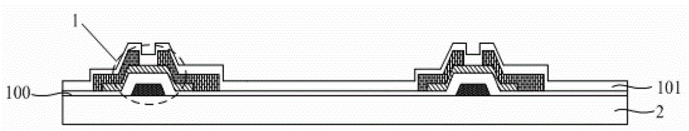
[0040] combine figure 1 As shown, a thin film transistor 1 is first formed on a base substrate 2 . Wherein, the base substrate 2 is made of a light-transmitting material with good light-transmitting properties, and is usually a glass substrate, a quartz substrate or a transparent resin substrate.

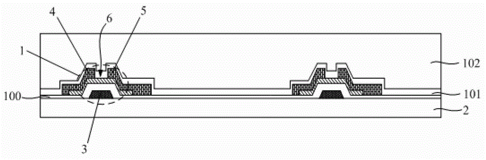
[0041] In one embodiment, forming the thin film transistor 1 on the base substrate 2 specifically includes: combining Figure 9 As shown, gate lines 20 and data lines 30 distributed horizontally and vertically are formed on the substrate 2, wherein the area defined by the crossing of gate lines 20 and data lines 30 is the pixel unit area 40, and the thin film transistor 1 is formed in the pixel unit area. In the region 40 , specifically, the thin film transistor 1 may be ...

Embodiment 2

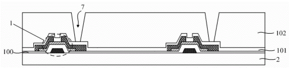
[0078] In this embodiment, an array substrate is provided, combined with Figure 8 and Figure 9 As shown, the array substrate includes a thin film transistor 1 formed on a base substrate 2 , a color filter 10 and a pixel electrode 9 , wherein the color filter 10 corresponds to the area where the pixel electrode 9 is located. The array substrate also includes a light-shielding sheet 8 formed on the top of the thin film transistor 1, and an opaque conductive metal layer film 103 of the same material as the light-shielding sheet 8 is provided above the passivation layer via hole 7, and the pixel electrode 9 passes through the opaque conductive metal layer. The thin film 103 is electrically connected to the drain electrode of the thin film transistor 1 . The setting of the light shield 8 can prevent the active layer of the thin film transistor 1 from being damaged due to excessive exposure in the patterning process, so as not to affect the characteristics of the thin film transi...

Embodiment 3

[0080] This embodiment provides a display device. The display device adopts the array substrate in Embodiment 2, forms the passivation layer via hole pattern through only one patterning process, and forms a The pattern of the light-shielding film, because the array substrate overcomes the damage to the active layer of the thin film transistor due to excessive exposure in the patterning process, thus will not affect the characteristics of the thin film transistor, and greatly reduces the cost of forming color filters on the array substrate. The cost is reduced, and the display quality of the display device is improved.

[0081]It can be seen from the above examples that the TFT array substrate and its manufacturing method and display device provided by the present invention form the passivation layer via hole pattern only through one patterning process, and then in the photoresist stripping process of the patterning process The pattern of the light-shielding sheet is formed, wh...


PUM


Abstract

Provided are a method for manufacturing a TFT array substrate, a TFT array substrate and a display device. The method comprises the following steps: S1. forming a thin-film transistor on an underlay substrate; S2. forming a passivation layer film on the underlay substrate completing step S1; S3. forming a pattern comprising a passivation layer via hole and a light-shield sheet on the underlay substrate completing step S2; and S4. forming a pattern of a colour filter and a pattern of a pixel electrode on the underlay substrate completing step S3, the pixel electrode being electrically connected to the drain electrode of the thin-film transistor via the passivation layer via hole, the colour filter corresponding to the pixel electrode in location.

Description

technical field [0001] The invention relates to the field of display technology, in particular to a TFT array substrate, a manufacturing method thereof, and a display device. Background technique [0002] Thin Film Transistor-Liquid Crystal Display (TFT-LCD) has the characteristics of small size, low power consumption, and no radiation. It has developed rapidly in recent years and occupies a dominant position in the current flat panel display market. The main structure of TFT-LCD includes the array substrate and the color filter substrate of the cell. A pixel matrix is ​​formed on the array substrate, and a thin film transistor (Thin Film Transistor, TFT for short) and a transparent pixel electrode are formed in each pixel area. The color filter substrate is formed with red, green, blue (R, G, B) color filters and black matrix composed of three color resins, wherein the black matrix is ​​set corresponding to the thin film transistor to prevent light leakage. The thin film ...

Claims


Application Information

Patent Timeline
Patent Type & Authority Patents(China)
IPC IPC(8): H01L21/77H01L27/12G02F1/1362G02F1/1368
CPCG02F1/1362H01L21/77H01L27/12G02F2001/136222G02F1/136227G02F1/136209H01L29/78633H01L27/1259G02F1/136222G02F1/1368H01L27/124H01L27/1288
Inventor 舒适惠官宝叶腾姜春生盖翠丽
Owner BOE TECH GRP CO LTD
Why Eureka
Try Eureka