Circuit structure for reducing input load of output driving module of LVDS (low voltage differential signaling) driver

An output drive, circuit structure technology, applied in logic circuits, electrical components, pulse technology, etc., to achieve the effect of simple structure, reduced load, and reduced input load

Active Publication Date: 2013-06-19
SOI MICRO CO LTD
View PDF3 Cites 8 Cited by
  • Summary
  • Abstract
  • Description
  • Claims
  • Application Information

AI Technical Summary

Problems solved by technology

The current consumption of the entire driver is

Method used


Image

  • Circuit structure for reducing input load of output driving module of LVDS (low voltage differential signaling) driver
  • Circuit structure for reducing input load of output driving module of LVDS (low voltage differential signaling) driver
  • Circuit structure for reducing input load of output driving module of LVDS (low voltage differential signaling) driver

Examples


Embodiment Construction

[0022] In order to make the object, technical solution and advantages of the present invention clearer, the present invention will be described in further detail below in conjunction with specific embodiments and with reference to the accompanying drawings.

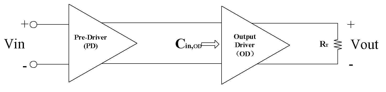
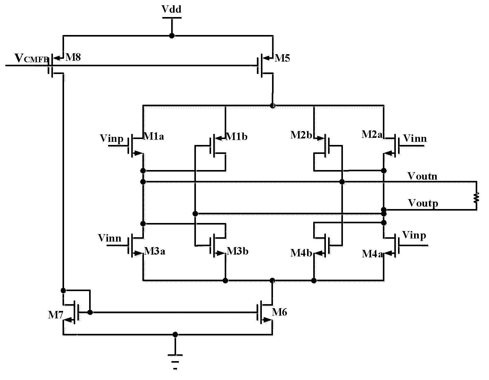
[0023] Such as figure 2 As shown, this circuit is an output driver module of a traditional LVDS driver. It is a common-mode feedback control unit composed of a CMOS transistor M8 and a CMOS transistor M5, and a mirror current source composed of a CMOS transistor M7 and a CMOS transistor M6. Transistors M1, M2, M3, and M4 form a current switch circuit, which controls current to flow through the load resistors in different directions, and then generates differential output signals at the output terminals Voutp and Voutn. Since the LVDS international standard stipulates that a current of 3.5 mA flows through the output resistor, the size of the current switch CMOS transistors M1 , M2 , M3 , and M4 is larger to allow a curr...


PUM


Abstract

The invention discloses a circuit structure for reducing the input load of an output driving module of a LVDS (low voltage differential signaling) driver. Vinn and Vinp are outputs of a pre-driving module of the LVDS driver and used for controlling four switching MOS (metal oxide semiconductor) transistors of the output driving module of the LVDS driver. Compared with a conventional LVDS driver circuit, the circuit structure has the advantages that the input load capacitance of the output driving module of the LVDS driver can be effectively reduced only by adding four switching MOS transistors without increasing any power consumption by a positive feedback shunt mechanism, namely, the output load capacitance of the pre-driving module is reduced, power consumption of a pre-driving portion of the LVDS driver is reduced, and accordingly, the performance of the whole driver is improved.

Description

technical field [0001] The invention relates to the technical field of Low-Voltage Differential Signaling (LVDS) driving composed of CMOS transistors, in particular to a circuit structure capable of effectively reducing the input load of an output driving module of an LVDS driver. Background technique [0002] With the rapid development and wide application of integrated circuits and microelectronics technology, transmission interface technology has become one of the research hotspots in the field of integrated circuits. As an interface technology with many advantages, LVDS transmission technology has gradually become one of the research hotspots. . [0003] Such as figure 1 As shown, the LVDS transmitter is generally divided into a pre-driver module (Pre-Driver, PD) and an output driver module (Output-Driver, OD). The role of the pre-driver module is to increase the driving capability of the signal, making it sufficient to drive the input load of the output driver module....

Claims


Application Information

Patent Timeline
Patent Type & Authority Applications(China)
IPC IPC(8): H03K19/094
Inventor 赵建中卜山刘海南黑勇周玉梅
Owner SOI MICRO CO LTD
Why Eureka
Try Eureka