Preparation method of metallic oxide thin film transistor

A technology of oxide thin films and transistors, applied in semiconductor/solid-state device manufacturing, electrical components, circuits, etc.

Inactive Publication Date: 2013-06-26
SHANGHAI UNIV
View PDF3 Cites 4 Cited by
  • Summary
  • Abstract
  • Description
  • Claims
  • Application Information

AI Technical Summary

Problems solved by technology

At present, flexible substrates (such as plastic substrates) cannot withstand temperatures above 300 ° C. Therefore, how to reduce the annealing temperature of thin films prepared by solution method is a research focus

Method used


Image

  • Preparation method of metallic oxide thin film transistor
  • Preparation method of metallic oxide thin film transistor
  • Preparation method of metallic oxide thin film transistor

Examples


Embodiment Construction

[0031] The embodiment of the present invention will be described in more detail below in conjunction with the accompanying drawings. This embodiment is implemented on the premise of the technical solution of the present invention, and the detailed embodiment and specific operation process are provided, but the protection scope of the present invention It is not limited to the following examples.

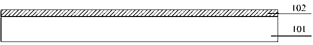
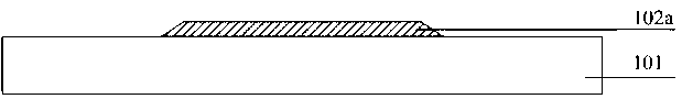
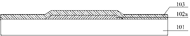
[0032] like Figure 1-Figure 9 As shown, a method for preparing a metal oxide thin film transistor has the following steps:

[0033] 1) On the cleaned glass substrate 101, the first conductive layer 102 is formed by radio frequency magnetron sputtering, and photoresist is coated on the first conductive layer 102; using the first mask plate, through exposure, Etching and stripping to form the gate electrode 102a;

[0034] 2) Depositing an insulating layer 103 on the gate electrode 102a by ion beam enhanced chemical vapor deposition;

[0035] 3) Prepare the solution. In this example...


PUM

PropertyMeasurementUnit
thicknessaaaaaaaaaa

Abstract

The invention discloses a preparation method of a metallic oxide thin film transistor. The preparation method includes: growing a first conducting layer on an insulating substrate, and photoetching to obtain a gate electrode; growing an insulating layer on the gate electrode; coating an active layer, and photoetching to obtain an active island; and depositing a second conducting layer, and photoetching to obtain a source electrode and a leakage electrode. By irradiating thin films prepared by a solution method, heat treatment temperature of the thin films can be lowered evidently, and metallic oxide can be formed at low temperature.

Description

technical field [0001] The invention relates to a method for preparing a metal oxide thin film transistor, belonging to the technical field of photoelectric display. Background technique [0002] Thin-film transistors (TFTs) are widely used as the core switching elements of active matrix display devices. At present, the TFT widely used in commercial flat panel displays is hydrogenated amorphous silicon TFT (a-Si:H TFT). <1cm 2 V -1 the s -1 ), hindering the development of high-performance flat-panel displays in the future. Although the polysilicon thin film crystal (Poly-Si TFT) tube has high mobility, due to its complicated process, low-temperature process is difficult to realize, which also limits the application of Poly-Si TFT. With the continuous development of AM-OLED and the demand for flexible display technology, there is a need for an active layer semiconductor material with high mobility and can be prepared at low temperature. As a new type of electronic dev...

Claims


Application Information

Patent Timeline
Patent Type & Authority Applications(China)
IPC IPC(8): H01L21/336
Inventor 李倩李喜峰信恩龙张建华
Owner SHANGHAI UNIV
Why Eureka
Try Eureka