Preparation method of TEM (transverse electric and magnetic field) sample

A sample and cross-section technology, applied in the field of TEM sample preparation, can solve the problems of inapplicability, affecting the process, bending and deformation of TEM samples, etc., to achieve the effect of improving quality, good physical hardness, and improving analysis quality

Active Publication Date: 2013-07-10
SHANGHAI HUALI MICROELECTRONICS CORP
View PDF8 Cites 22 Cited by
  • Summary
  • Abstract
  • Description
  • Claims
  • Application Information

AI Technical Summary

Problems solved by technology

[0007] However, this invention only cuts out two samples from the two areas to be tested of the test sample and sticks them together. If the thickness of the TEM that needs to be prepared is relatively thin, the prepared TEM sample is prone to bending and deformation, which will affect the subsequent process. It can be seen that, This invention is also not applicable in some semiconductor processes with smaller dimensions

Method used


Image

  • Preparation method of TEM (transverse electric and magnetic field) sample
  • Preparation method of TEM (transverse electric and magnetic field) sample
  • Preparation method of TEM (transverse electric and magnetic field) sample

Examples


Embodiment Construction

[0035] The present invention will be further described below in conjunction with the accompanying drawings and specific embodiments, but not as a limitation of the present invention.

[0036] Figure 1-8 It is a flow chart of a method for preparing a TEM sample of the copper seed crystal structure of the present invention, such as Figure 1-8 Shown, a kind of method for preparing the TEM sample of copper seed crystal structure specifically comprises the following steps:

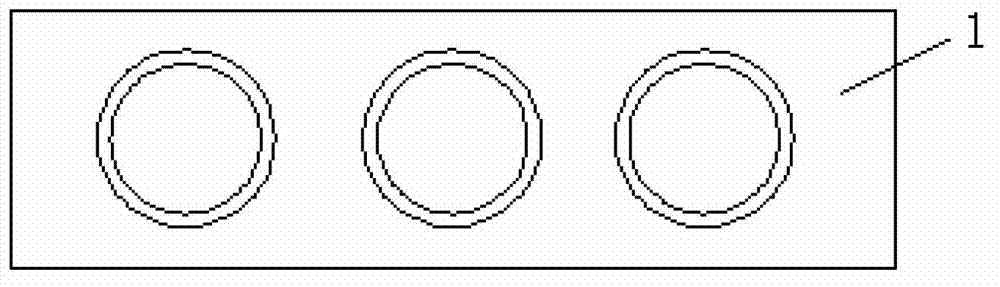
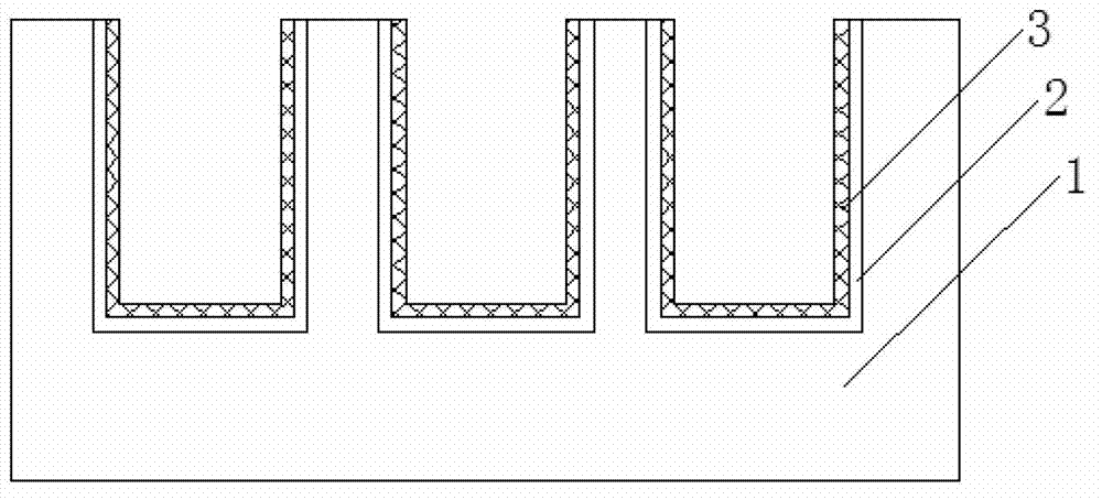
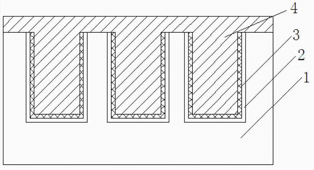
[0037] Step S1, providing a substrate 1 with a copper seed crystal structure, the trench is located in the substrate 1, the copper seed crystal structure includes a diffusion barrier layer 2 and a copper seed crystal layer 3, and the barrier layer 2 covers the bottom of the trench and its sidewall, the copper seed layer 3 covers the surface of the barrier layer 2, such as figure 1 and figure 2 The structure shown, where, figure 1 is a top view of a substrate with a copper seed structure, figure 2 is a ...


PUM

PropertyMeasurementUnit
thicknessaaaaaaaaaa

Abstract

The invention relates to the field of the manufacture of a semiconductor, and in particular relates to a preparation method of a TEM (transverse electric and magnetic field) sample. The preparation method comprises the following steps of: S1, depositing a first coating layer on the upper surface of a substrate; S2, cutting the first coating layer to the lower surface of the substrate; S3, preparing a second coating layer to cover the surface of a first cross section; S4, cutting the remaining first coating layer on a first sample structure to the lower surface of the remained substrate; S5, cutting the second coating layer to the lower surface of the remained substrate to form a TEM sample structure with a second cross section; and S6, continuously analyzing the target cross section of the TEM sample. According to the preparation method, a protection layer depositing method is improved, and the protection layer depositing time is increased, so that the thickness of the TEM sample can meet an optimal analysis thickness (40-60nm), a diffusion impervious layer and a copper interface can be clearly analyzed in the process of analysis, and the analysis quality of the TEM sample can be improved.

Description

technical field [0001] The invention relates to the field of semiconductor manufacturing, more precisely, to a method for preparing a TEM sample. Background technique [0002] With the continuous advancement of semiconductor technology, the size of samples becomes smaller and smaller. In some processes, material analysis of copper seed crystal structures is required. Therefore, the research on such structures and materials requires more and more precision processing. Capable focused ion beam system for TEM sample preparation. [0003] At present, the traditional method of using FIB (Focused Ion beam, focused ion beam) for TEM (Transmission electron microscope, transmission electron microscope) sample preparation is to deposit a layer of coating directly on the structure of the copper seed crystal, and then use FIB to prepare about The 10um wide target section is used for TEM analysis and observation. However, this preparation method is only suitable for the target surface ...

Claims


Application Information

Patent Timeline
Patent Type & Authority Applications(China)
IPC IPC(8): G01N1/28
Inventor 王炯翀
Owner SHANGHAI HUALI MICROELECTRONICS CORP
Why Eureka
Try Eureka