Gelatinized developing device with clustered structure

A technology of glue developing and equipment, which is applied in the direction of photo-engraving process coating equipment, electrical components, semiconductor/solid-state device manufacturing, etc., to achieve the effects of easy loading and disassembly, reduced machine footprint and strong technical expansion

Inactive Publication Date: 2013-07-10
SHENYANG KINGSEMI CO LTD
View PDF6 Cites 15 Cited by
  • Summary
  • Abstract
  • Description
  • Claims
  • Application Information

AI Technical Summary

Problems solved by technology

The above two types of structural equipment are still insufficient in terms of f

Method used


Image

  • Gelatinized developing device with clustered structure
  • Gelatinized developing device with clustered structure
  • Gelatinized developing device with clustered structure

Examples


Embodiment Construction

[0026] The present invention will be further described in detail below in conjunction with the accompanying drawings and embodiments.

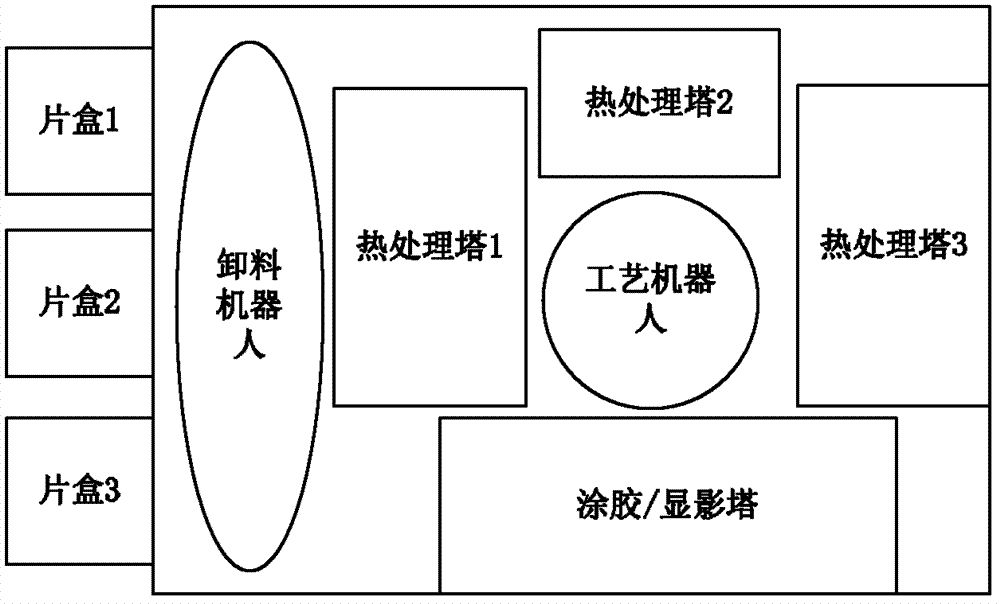
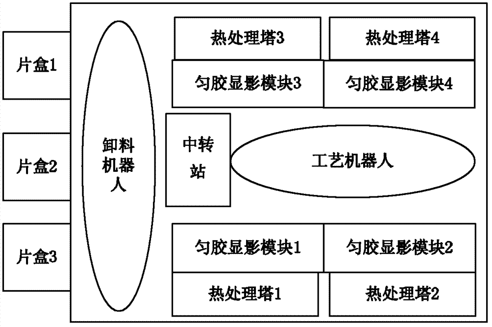
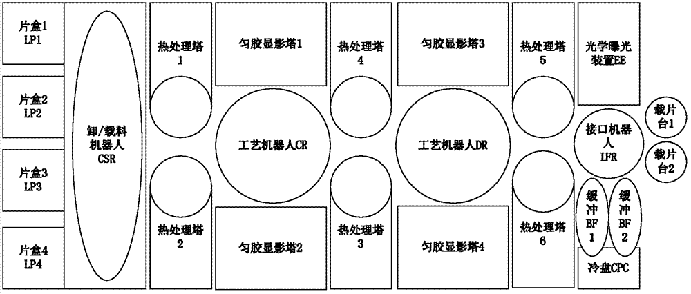
[0027] The structure of the present invention is as image 3 As shown, it includes cassette station, process station and interface station. The cassette station and process station transfer wafers through unloading / loading robots, and the process station and interface station transfer wafers through interface robots. Process stations include photoresist coating stations and developing station, the photoresist coating station and developing station are arranged in a line with the film cassette station and interface station, and the process processing modules in the station are distributed in clusters. DR; 4 heat treatment towers are arranged in four directions of the photoresist coating station, in counterclockwise order: heat treatment tower 1, heat treatment tower 2, heat treatment tower 3 and heat treatment tower 4, heat treatment tower 1 an...


PUM


Abstract

The invention relates to a structure of a gelatinized developing device, wherein the structure of the gelatinized developing device is used for achieving even-distributed photoresist and photoresist graphs in integrated circuit manufacture photolithography processing. The gelatinized developing device comprises a film magazine station, a process station and a connector station, wherein wafers are delivered between the film magazine station and the process station through an unloading/loading robot, the wafers are delivered between the process station and the connector station through a connector robot, the process station comprises a photoresist coating station and a developing station, the photoresist coating station and the developing station and the film magazine station and the connector station are arranged in a line, processing modules inside stations are in clustered distribution, and cluster origins are the processing robot CR and the processing robot DR and the processing robot CR and the processing robot DR are used for delivering the wafers inside the stations. The structure of the gelatinized developing device is small in occupied area of complete machine equipment, strong in technology development of the processing modules inside the process station and capable of enabling standardized modules to be easy to assemble and detach and enabling collocation and combination of the modules with different functions to be simple. Various production processes can be implemented on the gelatinized developing device.

Description

technical field [0001] The invention relates to the structure of a rubber coating and developing device used to obtain uniformly distributed photoresist and photoresist patterns on a semiconductor wafer in the photolithography process of integrated circuit manufacturing. Background technique [0002] At present, the photolithography process of semiconductor wafers is completed by the cooperation of photoresist coating machine, exposure machine and developing machine. The equipment manufacturers with advanced technology integrate the photoresist coating machine and developing machine into one glue coating machine. developing equipment. [0003] The gluing and developing equipment is mainly composed of a cassette station, a process station, and an interface station. The cassette station is responsible for loading wafers, feeding materials to the process station, receiving materials from the process station and sending them back to the cassette. The station is responsible for ...

Claims


Application Information

Patent Timeline
IPC IPC(8): H01L21/67G03F7/16G03F7/26
Inventor 胡延兵宗润福大谷正美王继周
Owner SHENYANG KINGSEMI CO LTD
Why Eureka
Try Eureka