Wafer level semiconductor encapsulation structure with stacking chips and manufacturing method thereof

A manufacturing method and semiconductor technology, applied in semiconductor/solid-state device manufacturing, semiconductor devices, semiconductor/solid-state device components, etc., can solve the problems of high cost of through-hole forming process, increase of product horizontal size and packaging structure, etc., to reduce product Dimensional and structural stress, the effect of saving packaging costs

Inactive Publication Date: 2013-07-10
ADVANCED SEMICON ENG INC
View PDF4 Cites 7 Cited by
  • Summary
  • Abstract
  • Description
  • Claims
  • Application Information

AI Technical Summary

Problems solved by technology

Among them, the method of arranging chips side by side will lead to a large increase in the horizontal size of the packaged product and its packaging structure will be affected by greater stress; Silicon via) manufacturing process, so that the upper chip can be electrically connected to the underlying circuit of the lower chip through the via hole, the disadvantage of this method is that the cost of the through hole forming process is too high

Method used


Image

  • Wafer level semiconductor encapsulation structure with stacking chips and manufacturing method thereof
  • Wafer level semiconductor encapsulation structure with stacking chips and manufacturing method thereof
  • Wafer level semiconductor encapsulation structure with stacking chips and manufacturing method thereof

Examples


Embodiment Construction

[0014] In order to make the above objects, features and advantages of the present invention more comprehensible, preferred embodiments of the present invention are exemplified below and described in detail in conjunction with the accompanying drawings. Furthermore, the directional terms mentioned in the present invention, such as "up", "down", "front", "back", "left", "right", "inside", "outside", "side", etc., It is only for orientation with reference to the attached drawings. Therefore, the directional terms used are used to illustrate and understand the present invention, but not to limit the present invention.

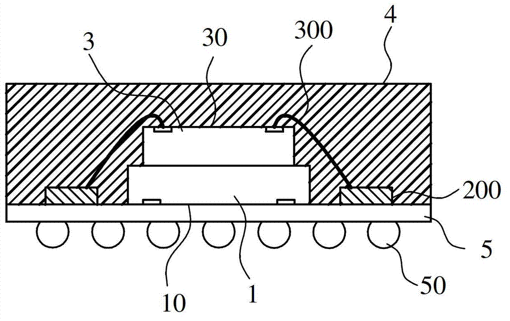
[0015] Please refer to figure 1 as shown, figure 1 It is a schematic structural view of a wafer-level semiconductor package structure with stacked chips according to an embodiment of the present invention. figure 1 The disclosed wafer-level semiconductor packaging structure with stacked chips mainly includes a first chip 1 , a plurality of lead frame terminals 2...


PUM


Abstract

The invention provides a wafer level semiconductor encapsulation structure with stacking chips and a manufacturing method of the wafer level semiconductor encapsulation structure. The wafer level semiconductor encapsulation structure comprises a first chip, a plurality of wire frame terminals, a second chip and encapsulation colloid, wherein the first chip is provided with a downward active surface, the wire frame terminals surround the first chip, the second chip is stacked on the first chip in an insulation mode and provided with an upward active surface, the active surface of the second chip is electrically connected to the wire frame terminals through metal wires, the encapsulation colloid covers the first chip, the wire frame terminals and the second chip, and the active surface of the first chip and the bottom faces of the wire frame terminals are exposed. According to the wafer level semiconductor encapsulation structure with the stacking chips, chip stacking is achieved through connection of the wire frame terminals and the metal wires, the size of a product and structural stress can be effectively reduced.

Description

technical field [0001] The invention relates to a semiconductor packaging structure, in particular to a wafer-level semiconductor packaging structure with stacked chips and a manufacturing method thereof. Background technique [0002] In the general wafer-level packaging manufacturing process, the packaging operation is performed directly on the wafer, and then the wafer is cut to complete the production of the semiconductor chip packaging structure. Since wafer-level packaging can complete all component assembly processes before wafer dicing, it can effectively reduce the cost of the entire product process cycle, and can achieve smaller-sized packaging to meet the requirements of light, thin and short, and its electrical connection On the one hand, it has shorter transmission lines, so wafer-level packaging is a packaging method that can effectively save space and cost. [0003] To meet design requirements, the current fan-out wafer-level (Fan out WLP) semiconductor packag...

Claims


Application Information

Patent Timeline
Patent Type & Authority Applications(China)
IPC IPC(8): H01L23/495H01L21/60
CPCH01L24/97H01L2224/48091H01L2924/15311H01L2224/97H01L21/568H01L24/96H01L2224/12105H01L2224/32145H01L2224/73267H01L2224/73265H01L2924/181H01L2224/19H01L2924/00014H01L2224/85H01L2924/00012H01L2224/83005
Inventor 唐和明洪志斌赵兴华刘昭源陈国华
Owner ADVANCED SEMICON ENG INC
Why Eureka
Try Eureka