

Semiconductor device and method for manufacturing semiconductor device
A semiconductor and device technology, applied in the fields of semiconductor/solid-state device manufacturing, semiconductor devices, electrical components, etc., can solve the problems of increasing electrode distance, increasing chip size, high cost, etc., and achieving the effect of high insulation withstand voltage
- Summary
- Abstract
- Description
- Claims
- Application Information
AI Technical Summary
Problems solved by technology
Method used
Image

Examples
no. 1 approach
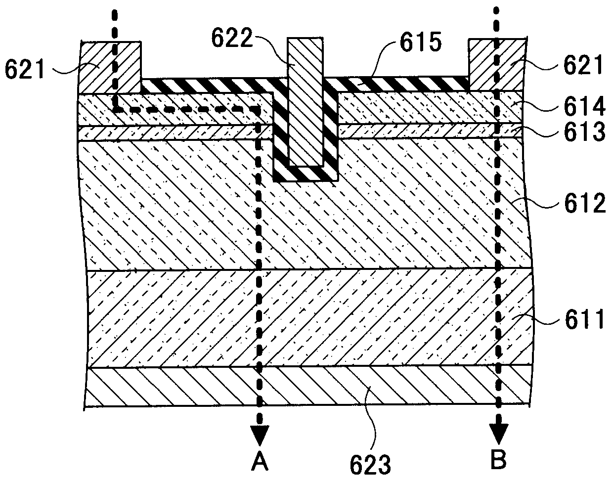
[0045] Semiconductor device
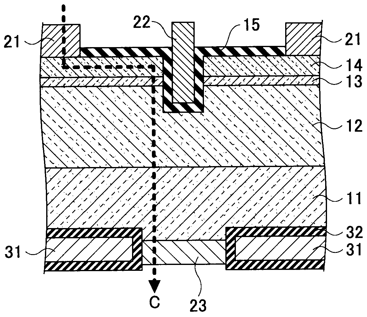
[0046] Next, the semiconductor device of this embodiment will be described. Such as figure 2 As shown, the semiconductor device of this embodiment is a field effect transistor with a vertical structure. Specifically, by n + - SiC or n + An n-GaN layer 12 , a p-GaN layer 13 , and an n-GaN layer 14 are formed on a substrate 11 made of GaN or the like, and an active electrode 21 is formed on a part of the surface of the n-GaN layer 14 . And, from the surface of the n-GaN layer 14, a part of the p-GaN layer 13 and the n-GaN layer 12 is etched to form an opening, and a gate insulating film 15 is formed, and the gate insulating film 15 is covered with The surface of the n-GaN layer 14 and the inner surface of the opening. A gate electrode 22 is formed in the opening with the gate insulating film 15 interposed therebetween.
[0047] Further, drain electrode 23 is formed on the back surface of substrate 11 , that is, on the side opposite to the sid...
no. 2 approach
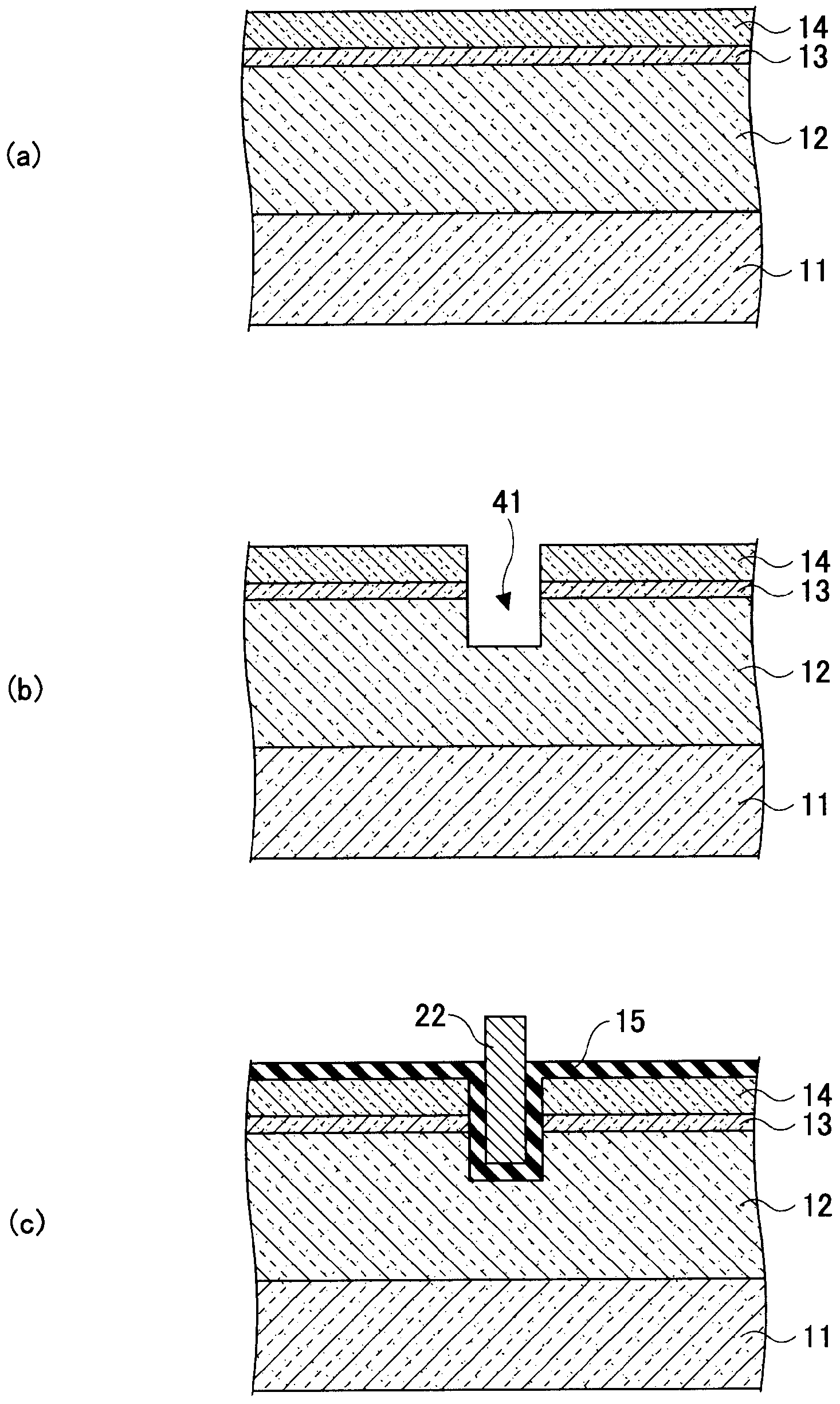
[0065] Next, the Figure 6 to Figure 8 , the method of manufacturing the semiconductor device according to the second embodiment will be described.
[0066] First, if Image 6 As shown in part (a), by the MOVPE method by n +- A buffer layer (not shown) is formed on a substrate 11 made of SiC, and an n-GaN layer 12 , a p-GaN layer 13 , and an n-GaN layer 14 are stacked on the buffer layer.
[0067] Next, if Image 6 As shown in part (b) of FIG. 2 , an opening 41 is formed in a region where a gate electrode 22 to be described later is to be formed.
[0068] Next, if Image 6 As shown in part (c), gate insulating film 15 is formed inside opening 41 and on the surface of n-GaN layer 14 , and gate electrode 22 is formed inside opening 41 via gate insulating film 15 .
[0069] Next, if Figure 7 As shown in part (a), the source electrode 21 is formed.
[0070] Next, if Figure 7 As shown in part (b) of FIG. Specifically, insulating film 132 made of SiN is formed to a thickn...
no. 3 approach
[0077] Next, the Figure 9 to Figure 11 , the method of manufacturing the semiconductor device according to the third embodiment will be described.
[0078] First, if Figure 9 As shown in part (a), by the MOVPE method, come in by n +- A buffer layer (not shown) is formed on a substrate 11 made of SiC, and an n-GaN layer 12 , a p-GaN layer 13 , and an n-GaN layer 14 are stacked on the buffer layer.
[0079] Next, if Figure 9 As shown in part (b) of FIG. 2 , an opening 41 is formed in a region where a gate electrode 22 to be described later is to be formed.
[0080] then, Figure 9 As shown in part (c), gate insulating film 15 is formed inside opening 41 and on the surface of n-GaN layer 14 , and gate electrode 22 is formed inside opening 41 via gate insulating film 15 .
[0081] Next, if Figure 10 As shown in part (a), the source electrode 21 is formed.
[0082] Next, if Figure 10 As shown in part (b) of the substrate 11, a part of the region other than the region c...
PUM
| Property | Measurement | Unit |
|---|---|---|
| Thickness | aaaaa | aaaaa |
Abstract
Description
Claims
Application Information