

Wafer processing jig
A jig and wafer technology, which is applied in the direction of electrical components, semiconductor/solid-state device manufacturing, circuits, etc., can solve problems such as difficulty in ensuring stability and wafer processing quality, and achieve reduced production costs, consistent state, and Consistent results in processing quality
- Summary
- Abstract
- Description
- Claims
- Application Information
AI Technical Summary
Problems solved by technology
Method used
Image

Examples
Embodiment Construction
[0028] In order to make the technical means, creative features, goals and effects achieved by the present invention easy to understand, the present invention will be further described below in conjunction with specific diagrams.
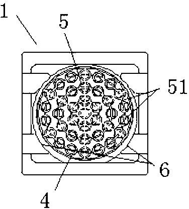
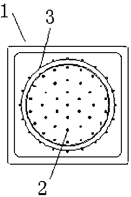
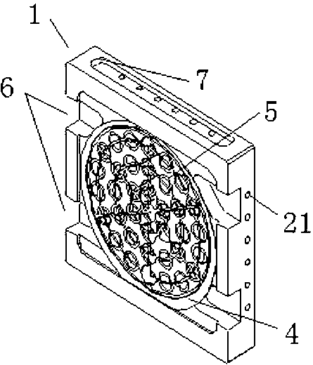
[0029] refer to figure 2 , image 3 , a wafer processing fixture, including a carrying platform 1, an adsorption mechanism is arranged on the carrying platform 1, and the adsorption mechanism includes a plurality of adjusting adsorption holes 2 arranged in the middle of the carrying platform 1 and a plurality of suction holes arranged on the periphery of the carrying platform 1 A fixed adsorption hole 3. A plurality of fixed adsorption holes 3 are arranged on the carrying platform 1 in a circular shape, and a plurality of adjustable adsorption holes 2 are arranged inside the fixed adsorption holes 3 . A plurality of fixed adsorption holes 3 are connected to a fixed suction device through gas passages. The plurality of adjustable adsorption holes ...
PUM
 Abstract
Description
Claims
Application Information