

Optical detector based on two-dimensional stratiform atomic crystal materials
A two-dimensional layered, crystalline material technology, applied in semiconductor devices, electrical components, circuits, etc., can solve the problems of difficult to achieve ultrafast broadband absorption photodetectors, difficult to extract photogenerated carriers, and low photoresponsivity of devices , to achieve the effect of improving directional movement and extraction, improving device responsivity, and high device success rate
- Summary
- Abstract
- Description
- Claims
- Application Information
AI Technical Summary
Problems solved by technology
Method used
Image

Examples
Embodiment Construction
[0029] The present invention will be described in detail below with reference to the accompanying drawings and in combination with embodiments.
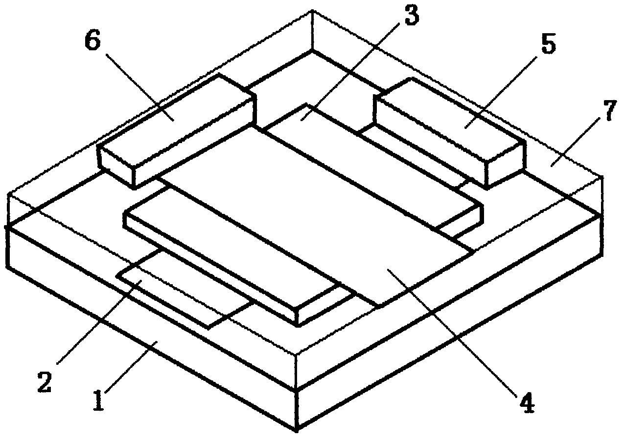
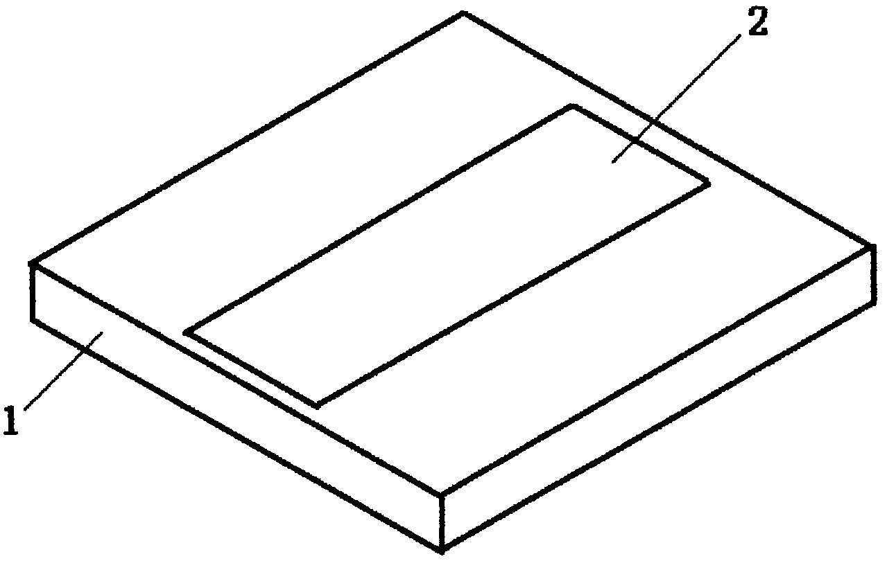
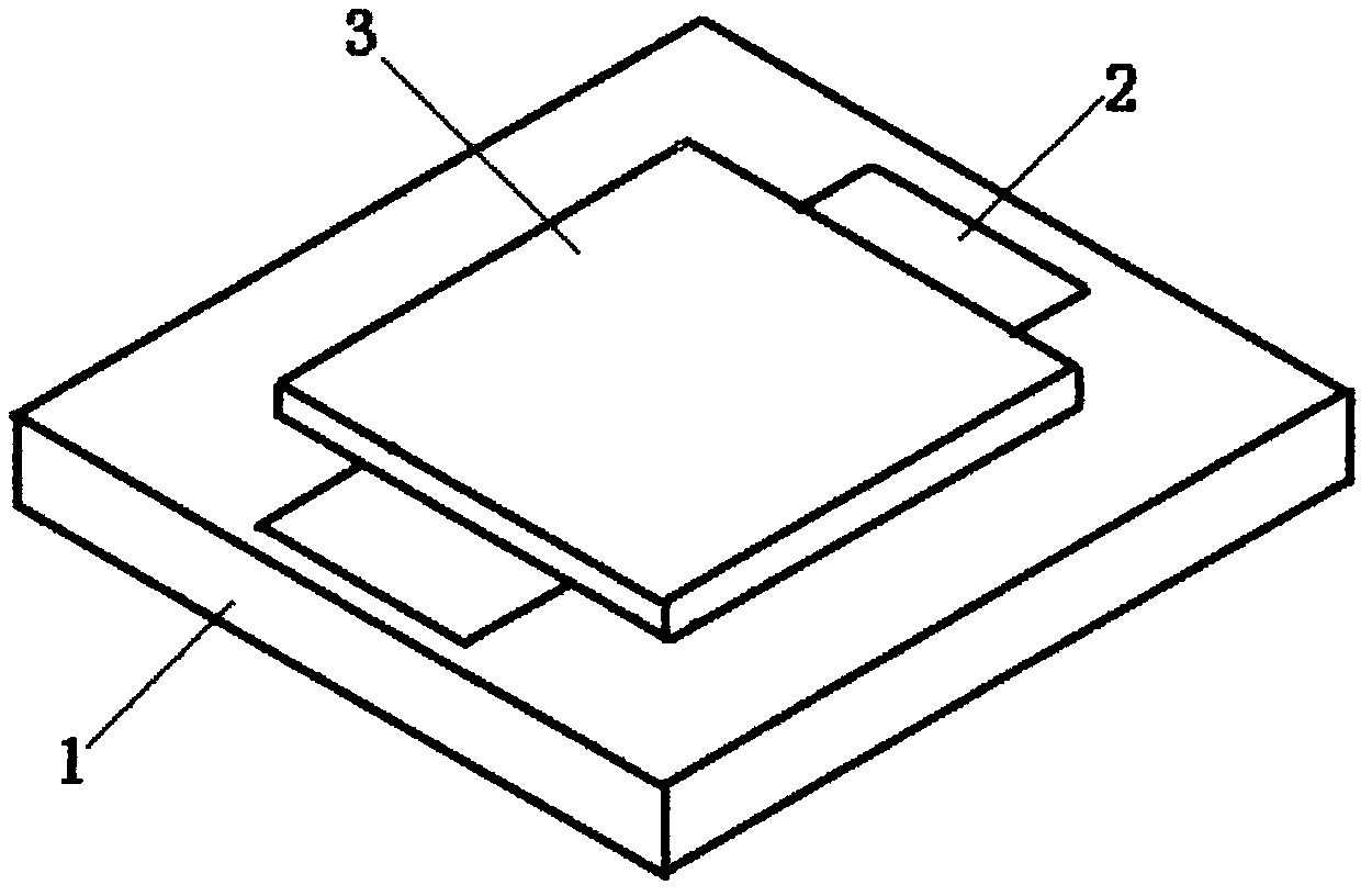
[0030] see figure 1 As shown, a photodetector based on a two-dimensional layered atomic crystal material includes a silicon substrate 1 covered by silicon dioxide, and the silicon substrate 1 covered by silicon dioxide is sequentially superimposed and covered with a first graphene conductive layer 2. A two-dimensional layered atomic crystal semiconductor material layer 3 and a second graphene conductive layer 4, the first graphene conductive layer 2 and the second graphene conductive layer 4 are respectively connected with the two-dimensional layered atomic crystal The semiconductor material layer 3 forms a heterojunction structure; one end outside the overlapping area of the first graphene conductive layer 2 and the two-dimensional layered atomic crystal semiconductor material layer 3 and the second graphene conductive layer 4 A ...
PUM
| Property | Measurement | Unit |
|---|---|---|
| Thickness | aaaaa | aaaaa |
Abstract
Description
Claims
Application Information