Bipolar non-punch-hrough power semiconductor device

A semiconductor and power-through technology, which is applied in the field of bipolar non-through power semiconductor devices and manufactures such power semiconductor devices, can solve problems such as slowness and high loss, and achieve the goals of reducing thermal budget, short diffusion time, and saving thermal budget Effect

Active Publication Date: 2013-07-24
HITACHI ENERGY SWITZERLAND AG
View PDF14 Cites 6 Cited by
  • Summary
  • Abstract
  • Description
  • Claims
  • Application Information

AI Technical Summary

Problems solved by technology

[0007] Since this angle (at which the thickness of the edge layer 50, 60 decreases) is small (approximately 2°) in order to slowly reduce the electric field towards the lateral edge...

Method used


Image

  • Bipolar non-punch-hrough power semiconductor device
  • Bipolar non-punch-hrough power semiconductor device
  • Bipolar non-punch-hrough power semiconductor device

Examples


Embodiment Construction

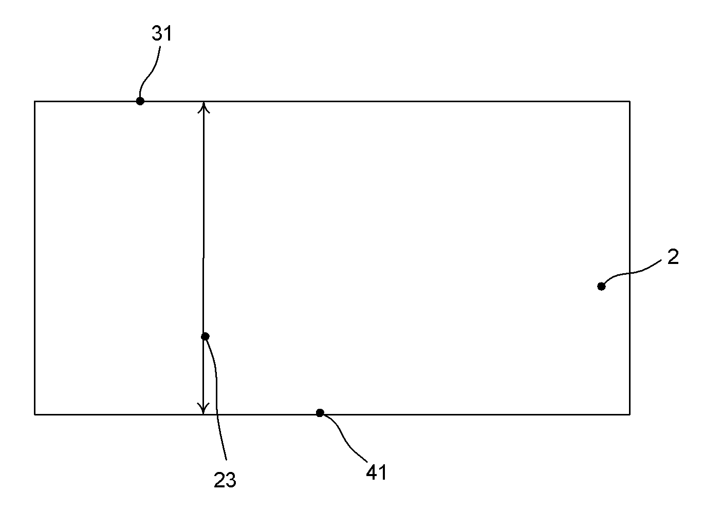
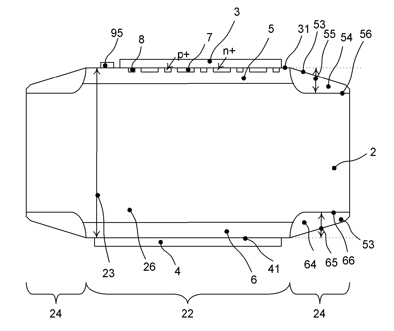
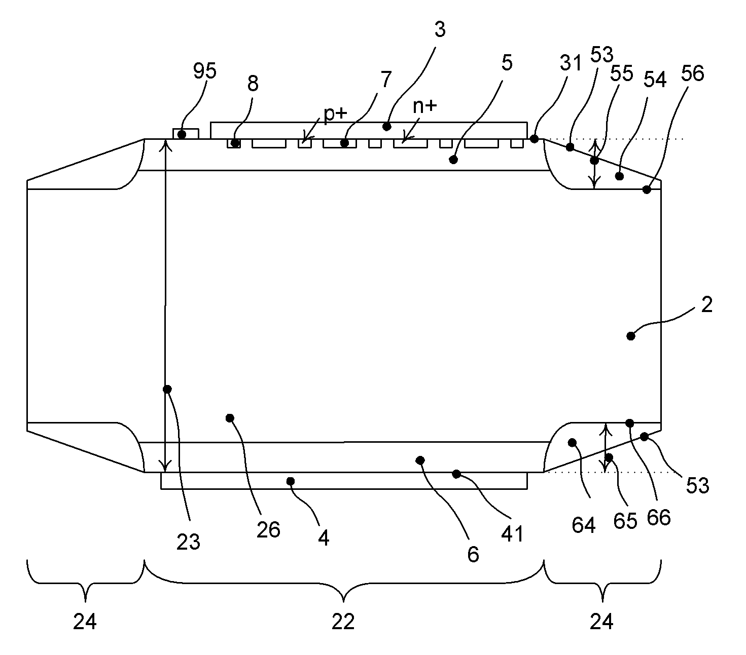
[0041] A bipolar non-punch-through power semiconductor arrangement according to the invention in the form of a phase-controlled thyristor (PCT) 1 with a blocking voltage of at least 1000 V is shown in FIG. 2 . The device comprises a semiconductor wafer 2 having layers of different conductivity types on which a cathode contact 3 is formed on a cathode side 31 of the wafer and an anode contact 4 is formed on an anode side 41 of the wafer opposite to the cathode side 31 . An (n-)doped drift layer 26 is formed in the wafer. A p-doped base layer 5 is arranged on this drift layer 26 towards the cathode side 31 . It touches the cathode contact 3. The base layer 5 is arranged directly adjacent to the drift layer 26 , which means that no further intermediate layers of the second conductivity type are arranged between the base layer 5 and the drift layer 26 . The base layer 5 and the drift layer 26 are connected to each other, ie they touch each other. The base layer 5 extends in the...


PUM


Abstract

A bipolar non-punch-through power semiconductor device is provided. It comprises a semiconductor wafer (2) and a first electrical contact on a first main side and a second electrical contact on a second main side. The wafer (2) comprises an inner region (22) with a wafer thickness (23) and a termination region (24), which surrounds the inner region (22) and in which the wafer thickness (23) is reduced at least on the first main side with a negative bevel. The semiconductor wafer (2) comprises at least a two-layer structure with layers of different conductivity types: - a drift layer (26) of a first conductivity type, a first layer of a second conductivity type directly connected to the drift layer (26) on the first main side and contacting the first electrical contact, which first layer extends to a first layer depth, and - a second layer of the second conductivity type, which is arranged in the termination region (24) on the first main side up to a second layer depth. The second layer depth is larger than the first layer depth, which first layer depth is at most 45 [mu]m. The doping concentration of the second layer is lower than the doping concentration of the first layer.

Description

technical field [0001] The invention relates to the field of power electronics and more particularly to a bipolar non-punch-through power semiconductor arrangement according to the preamble of claim 1 and a method for manufacturing such a power semiconductor arrangement. Background technique [0002] No. 5,710,442 describes a phase-controlled thyristor (PCT) 10 having a wafer 2 on which a cathode contact 3 is arranged on a cathode side 31 . The anode contact 4 is formed on the anode side 41 of the wafer opposite the cathode side 31 . Inside the wafer 2 a (n−)-doped drift layer 26 is arranged. A p-doped base layer 5 is provided on this drift layer 26 towards the cathode side 31 , which contacts the cathode contact 3 . The (N+) doped cathode layer 7 and the (p+) short region 8 are embedded in the base layer 5 . They also contact the cathode electrode 3 . Transverse to cathode contact 3 and separated therefrom by drift layer 26 is arranged gate contact 95 . [0003] Arrang...

Claims


Application Information

Patent Timeline
IPC IPC(8): H01L29/06H01L29/747H01L29/87H01L29/861H01L21/329
CPCH01L29/0661H01L29/102H01L29/8613H01L29/0615H01L29/74H01L29/0834H01L29/66136H01L29/0619H01L29/66363H01L29/7432H01L29/87H01L29/06H01L29/747
Inventor J.福贝基M.拉希莫
Owner HITACHI ENERGY SWITZERLAND AG
Why Eureka
Try Eureka