SPR phase measurement method for measuring thickness of nano metal film

A metal thin film and phase measurement technology, applied in the direction of measuring devices, optical devices, instruments, etc., can solve the problems of thin film sample damage, damage to sample integrity, high price, etc., and achieve the effect of easy operation

Inactive Publication Date: 2013-07-31
TIANJIN UNIV
View PDF3 Cites 26 Cited by
  • Summary
  • Abstract
  • Description
  • Claims
  • Application Information

AI Technical Summary

Problems solved by technology

However, the high-precision microscope has a complex structure, is expensive, and is not easy to operate. The contact

Method used


Image

  • SPR phase measurement method for measuring thickness of nano metal film
  • SPR phase measurement method for measuring thickness of nano metal film
  • SPR phase measurement method for measuring thickness of nano metal film

Examples


Embodiment Construction

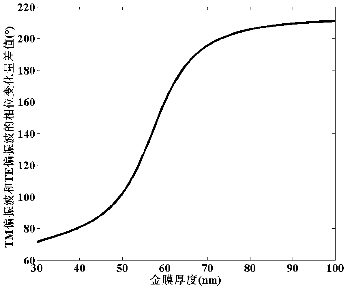
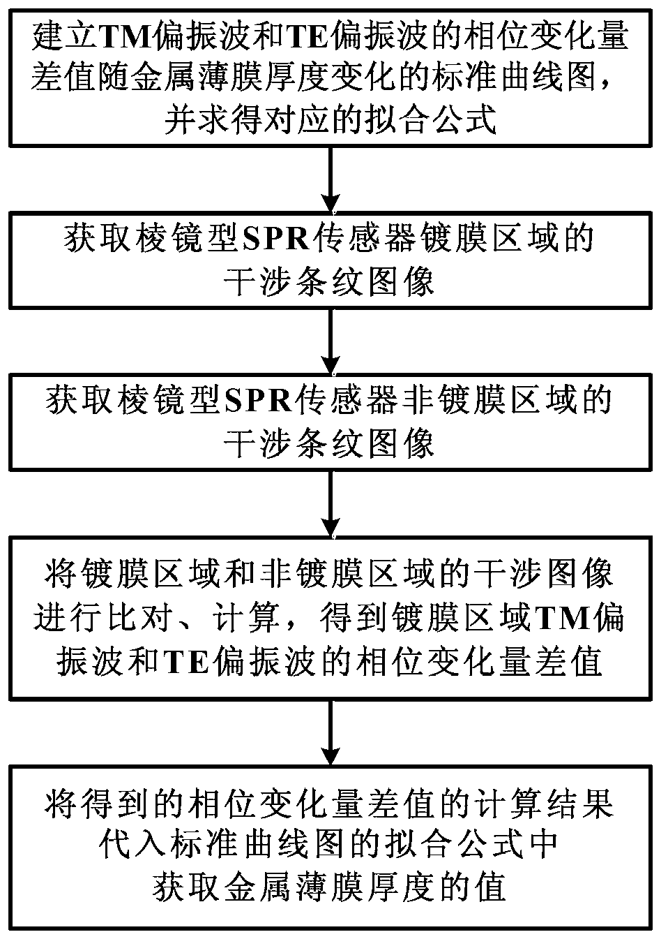
[0028] Below in conjunction with accompanying drawing and specific embodiment the present invention is described in further detail:

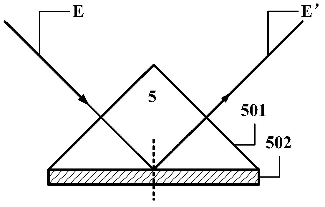
[0029] The surface plasmon resonance (Surface Plasmon Resonance, SPR) effect is a special physical optics phenomenon. The evanescent wave generated when the light wave is totally reflected at the interface between the medium and the metal can trigger the collective oscillation of the free electrons on the metal surface, thus forming a surface plasmon wave (Surface Plasmon Wave, SPW), whose magnetic field vector direction is parallel At the interface between the medium and the metal, the magnetic field intensity reaches the maximum at the interface and shows an exponential decay trend in the two media. When the wave vector of the incident light is equal to the wave vector of the surface plasmon wave, the SPR effect can be excited. At present, the modulation types of SPR sensing technology mainly include angle type, spectral type and phase type. A...


PUM


Abstract

The invention relates to an SPR (surface plasmon resonance) phase measurement method for measuring thickness of a nano metal film. The method comprise the steps of 1, establishing a standard curve graph of the variation of a phase variation difference of a TM polarized wave and a TE polarized wave with the thickness of the metal film, and obtaining a corresponding fitting formula, 2, obtaining a coating interference fringe image of a film coating area of a prism SPR sensor, 3, obtaining an interference fringe image of a non-film coating area of the prism SPR sensor, 4, comparing and calculating the images obtained in Step 2 and Step 3, and obtaining the phase variation difference of the TM polarized wave and the TE polarized wave in the film coating area, and 5, substituting a calculated result in Step 4 into the fitting formula of the standard curve graph in Step 1, and obtaining a value of the thickness of the metal film. The SPR phase measurement method has the benefits that phase modulation is conducted on the TM polarized wave and the TE polarized wave by laser interference, so that non-contact, high-precision and convenient-to-operate measurement of the thickness of the nano metal film can be achieved.

Description

technical field [0001] The invention relates to a method for measuring the thickness of a metal thin film, in particular to an SPR phase measurement method for measuring the thickness of a nanoscale metal thin film. Background technique [0002] With the wide application of thin film technology in the fields of microelectronics, optoelectronics, aerospace, bioengineering, weaponry, food science, medical equipment and polymer materials, thin film technology has become a research hotspot in the field of current scientific and technological research and industrial production. In particular, the rapid development of nanoscale thin film technology has directly affected the development direction of science and technology and people's way of life. The continuous improvement and rapid development of thin-film manufacturing technology also put forward higher requirements for various parameters of the thin film, such as the refractive index and thickness parameters of the thin film, a...

Claims


Application Information

Patent Timeline
IPC IPC(8): G01B11/06
Inventor 刘庆钢刘超樊志国刘士毅陈良泽梁君
Owner TIANJIN UNIV
Why Eureka
Try Eureka