Photonic crystal-based integratable quantum walking device

A technology of photonic crystals and quantum walks, applied in optical components, light guides, optics, etc., can solve problems such as slow light effects, affecting light field coupling and interference, differences, etc., to achieve optimized device design, simple and clear relationships, and beneficial to photons integrated effect

Active Publication Date: 2013-08-07
INST OF SEMICONDUCTORS - CHINESE ACAD OF SCI
View PDF3 Cites 3 Cited by
  • Summary
  • Abstract
  • Description
  • Claims
  • Application Information

AI Technical Summary

Problems solved by technology

First of all, its principle of light field confinement can be explained by Bragg reflection. The light field is often effectively extended to four or more rows of photonic crystal holes, and the change of the number of air hole rows between coupling elements will greatly affect the coupling of the light field. and interference; secondly, the waveguide mechanism of the photonic crystal waveguide is different from that of ordinary waveguides. When the photons are guided in it, they may be reflected many times, resulting in the so-called slow light effect; finally, the scattering of photons by the photonic crystal holes can lead to randomness. stronger walking
These properties make quantum walks in photonic crystals very different from walks in ordinary waveguides

Method used


Image

  • Photonic crystal-based integratable quantum walking device
  • Photonic crystal-based integratable quantum walking device
  • Photonic crystal-based integratable quantum walking device

Examples


Embodiment 1

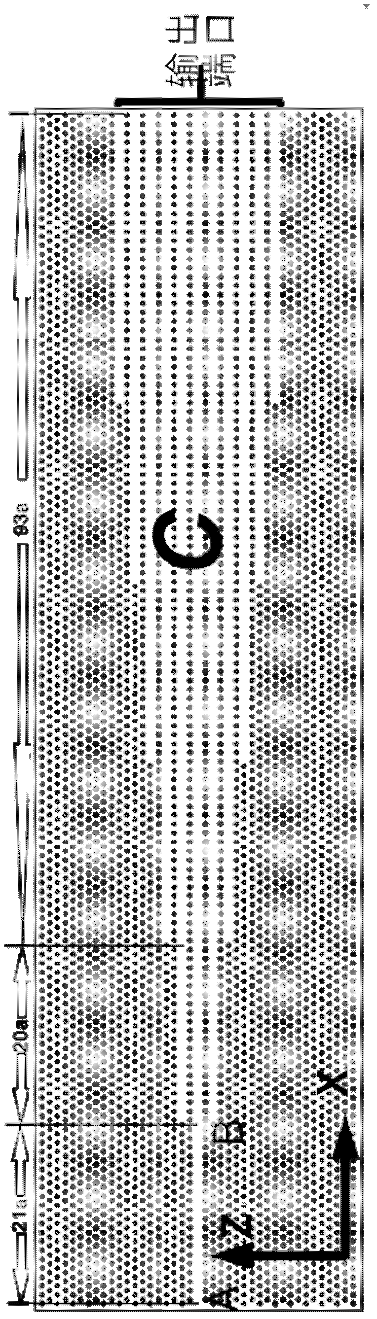
[0032] (a) in FIGS. 2 to 5 shows the structure of a photonic crystal quantum walker coupled waveguide array in the present invention. As shown in (a) of Figures 2-5, the photonic crystal has a hexagonal lattice air hole structure, the dark part in the figure is the air hole, and the light part is silicon. In a photonic crystal with a complete lattice, every other row or several rows of air holes is removed to form a coupled waveguide array. The distance between the photonic crystal waveguides obtained in this way is small, and light can be coupled between adjacent waveguides.

[0033] Figure 2(a) , 3(a) The length of the photonic crystal waveguide is gradual, the photonic crystal period is 405 nanometers, and the air hole radius is 0.28×photonic crystal period. In the figure, AB is the input waveguide with a certain length, and the coupling region (C) also has a certain length. It should be noted that there are no special requirements for the length of the input waveguide,...

Embodiment 2

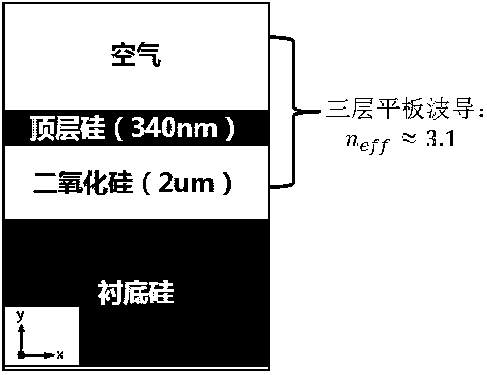
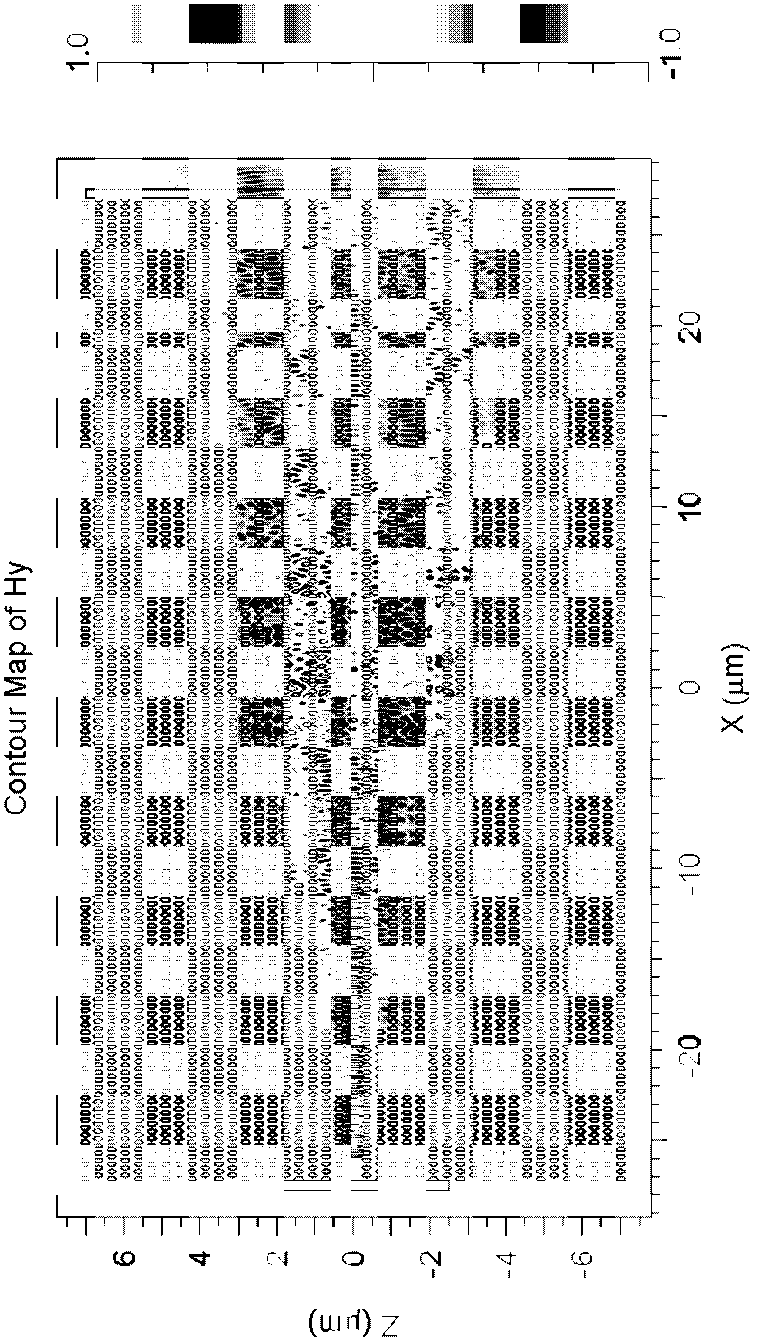
[0046] Fig. 6(a) and Fig. 7(a) show the structure of another quantum walking device—coupling microcavity array. use figure 1 In the three-layer flat plate structure, the hexagonal lattice air hole photonic crystal period is 420 nm, and the air hole radius is 0.32×photonic crystal period. The input waveguide AB is a special Γ-M waveguide, which is convenient to match with the microcavity array to reduce reflection. In a photonic crystal with a complete lattice, the coupled microcavity array can be obtained by removing the air holes one by one according to a certain lattice rule, in which each air hole corresponds to a point in the lattice. Figure 6(a) and 7(a) The lattice used in the structure is formed by the arrangement of equilateral triangles according to two different rules. Figure 6(a) and 7(a) The size of the overall device is 16×13.8um in turn 2 and 25.6×10.9um 2 , are on the order of tens of microns.

[0047] Again, the selected photonic crystal period, the si...


PUM


Abstract

The invention discloses a photonic crystal-based integratable quantum walking device. By utilizing the limit characteristic of photonic crystal to light fields, intercoupling and interference among the light fields of a wider range are realized, so that quantum walking of photons is realized on an integrated optical device of which the dimension is extremely small. The invention belongs to the field of semiconductor integrated optical technology and the quantum information science.

Description

technical field [0001] The invention relates to the fields of semiconductor integrated optics technology and quantum information science, in particular to an integrable quantum device based on photonic crystals. Background technique [0002] Quantum information science is an emerging discipline that uses quantum effects to process and transmit information. As the core of quantum information processing, quantum computing has gradually attracted widespread attention from the idea of ​​quantum computer proposed by Feynman et al. to the quantum Shor algorithm. The classical algorithm based on classical random walk has been very mature and widely used, but there are only a handful of existing quantum algorithms, and the construction of a complete quantum algorithm has become the key to realizing large-scale quantum computing and quantum computers. In the 1990s, people began to study quantum walks, began to use quantum walks to construct new quantum algorithms, and also used quan...

Claims


Application Information

Patent Timeline
IPC IPC(8): G02B6/122
Inventor 郑婉华祁帆冯志刚王宇飞
Owner INST OF SEMICONDUCTORS - CHINESE ACAD OF SCI
Why Eureka
Try Eureka