
Segmentation laser punching method

A laser drilling and laser beam technology, applied in the field of microelectronics, can solve problems such as hole shape distortion and reduce drilling accuracy, and achieve the effects of uniform aperture, reduced ablation ability, and improved drilling accuracy

Active Publication Date: 2015-02-11
NO 54 INST OF CHINA ELECTRONICS SCI & TECH GRP
View PDF7 Cites 0 Cited by
  • Summary
  • Abstract
  • Description
  • Claims
  • Application Information

AI Technical Summary

Problems solved by technology

[0003] At present, the commonly used laser drilling mainly adopts the method of one-time forming for drilling. When the hole depth is large, the steam ejected from the hole will produce irregular shielding and scattering of the laser beam, causing the distortion of the hole shape and reducing the drilling efficiency. Hole precision

Method used


Image

  • Segmentation laser punching method

Examples


Embodiment 1

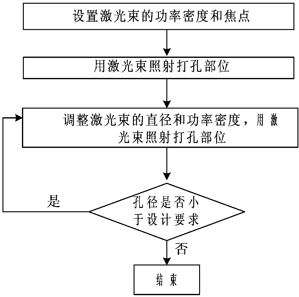
[0020] Step 1: Focus the laser beam on the drilled part of the crystalline silicon.

[0021] Adjust the power density of the laser beam to 10 8 W / cm 2 , After the diameter is adjusted to 20um, focus on the center of the punched part. The wavelength of the ultraviolet laser beam is 355nm-266nm.

[0022] Step 2: Irradiate the laser beam to the perforated part for 0.0001s.

[0023] Step 3: After reducing the diameter of the laser beam by 3% and increasing the power density by 2%, irradiate the perforated part for 0.0001s.

[0024] Adjust the power density of the laser beam to 1.02*10 8 W / cm 2 , After the diameter is adjusted to 19.4um, focus on the center of the punched part, and irradiate the punched part for 0.0001s.

[0025] Step 4: On the basis of reducing the diameter by 3% and increasing the power density by 2% in the previous step, further reduce the diameter of the UV-level ultraviolet laser beam by 3% and increase the power density by 2%. Part 0.0001s-0.1s; after ...

Embodiment 2

[0037] Step A: Focus the laser beam on the drilled part of the crystalline silicon.

[0038] Adjust the power density of the laser beam to 10 8 W / cm 2 , After the diameter is adjusted to 20um, focus on the center of the punched part.

[0039] Step B: irradiate the laser beam to the perforated part for 0.0002s.

[0040] Step C: After reducing the diameter of the laser beam by 3% and increasing the power density by 2%, irradiate the perforated part for 0.0002s.

[0041] Adjust the power density of the laser beam to 1.02*10 8 W / cm 2 , After the diameter is adjusted to 19.4um, focus on the center of the punched part, and irradiate the punched part for 0.0002s.

[0042] Step D: On the basis of reducing the diameter by 3% and increasing the power density by 2% in the previous step, further reduce the diameter of the UV-level ultraviolet laser beam by 3% and increase the power density by 2%, and then irradiate Part 0.0001s; after that, go to step E;

[0043] Step E: If the dep...


PUM

PropertyMeasurementUnit
wavelengthaaaaaaaaaa

Abstract

The invention discloses a segmentation laser punching method mainly solving the problem that diameters of punched holes by the existing laser punching technology is not uniform. The segmentation laser punching method mainly comprises the following steps of adjusting the power density of ultraviolet light laser beams with the wavelength 266 nm to 355 nm to be larger than 107 W / cm<2> and accurately focusing the ultraviolet light laser beams to punching positions of punching materials; enabling the ultraviolet light laser beams to irradiate the punching positions for 0.0001 to 0.1 s; progressively enabling the diameters of the ultraviolet light laser beams to be reduced by 1 to 6% and the power of the ultraviolet light laser beams to be increased by 0.5 to 4% and the punching positions to be irradiated for 0.0001 to 0.1 s repeatedly; and stopping punching until the hole depth meets design requirements. The segmentation laser punching method which employs a segmentation way for punching has the advantages of enabling the energy of the ultraviolet light laser beams to be reduced, the depth of holes to be increased and the deviation of the holes to be reduced, accordingly enabling the accuracy of the holes to be significantly improved, and expending the application range of laser punching.

Description

technical field [0001] The invention belongs to the technical field of microelectronics, and relates to the design of a semiconductor material and a preparation method thereof, in particular to a segmented laser drilling method. Background technique [0002] Laser drilling uses a laser beam as a heat source to melt and vaporize the material to be removed. Laser beam is a highly concentrated photon beam in time and space, with extremely small divergence angle and good focusing performance. The optical focusing system is used to focus the laser beam to the range of micron. When the laser beam irradiates the silicon wafer, the temperature in the irradiation area rises to over 10,000 degrees instantly, and the silicon material in the irradiation area melts and evaporates instantaneously. , the air pressure rises sharply, and the high-speed airflow violently ejects outward, forming a small pit immediately on the irradiation point. With the continuous input of laser energy, the ...

Claims


Application Information

Patent Timeline
Patent Type & Authority Patents(China)
IPC IPC(8): B23K26/382
Inventor 甄立东赵永瑞梁栋毕明路米新泉田磊
Owner NO 54 INST OF CHINA ELECTRONICS SCI & TECH GRP
Learn More