Solid-state image sensing device

A sensing device and solid-state image technology, applied in image communication, electric solid-state devices, television, etc., can solve the problems of large circuit scale and no description

Active Publication Date: 2013-08-14
CANON KK
View PDF7 Cites 7 Cited by
  • Summary
  • Abstract
  • Description
  • Claims
  • Application Information

AI Technical Summary

Problems solved by technology

[0004] However, for the method using multiple comparators described in Document 1, the circuit scale is large
Furthermore, Document 2 does not describe a method of supplying a plurality of reference signals when comparing a pixel signal with a reference signal that has been selected from a plurality of reference signals each having a ramp voltage

Method used


Image

  • Solid-state image sensing device
  • Solid-state image sensing device
  • Solid-state image sensing device

Examples


no. 1 example

[0040] [installation layout]

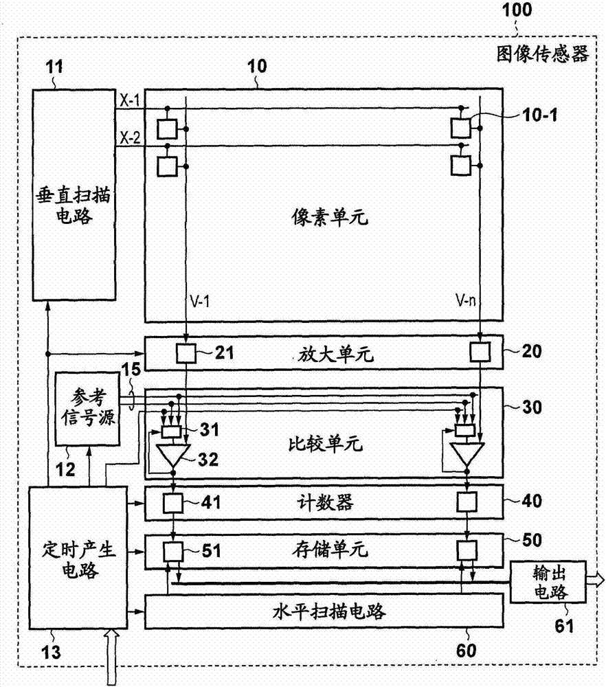
[0041] will refer to figure 1 The circuit diagram shown in describes the arrangement of an image sensor 100 used as a solid-state image sensing device according to one embodiment. The image sensor 100 will be referred to as a CMOS image sensor, which performs photoelectric conversion on a subject image obtained by receiving light and outputs an electrical signal as a digital signal. The image sensor 100 includes the following main circuit blocks.

[0042] The pixel unit 10 functions as a photoelectric conversion region. The vertical scanning circuit 11 scans the pixel unit 10 . The amplification unit 20 amplifies the analog pixel signal output from the pixel unit 10 . The reference signal source 12 functions as a reference signal generating unit that generates a reference signal having a ramp voltage or the like.

[0043] The comparison unit 30 compares the pixel signal with a reference signal. The counter 40 counts the comparison period of...

no. 2 example

[0071] A solid-state image sensing device and an A / D conversion method therefor according to a second embodiment of the present invention will be described below. Note that in the second embodiment, the same components as those in the first embodiment have the same reference numerals, and a detailed description thereof will be omitted.

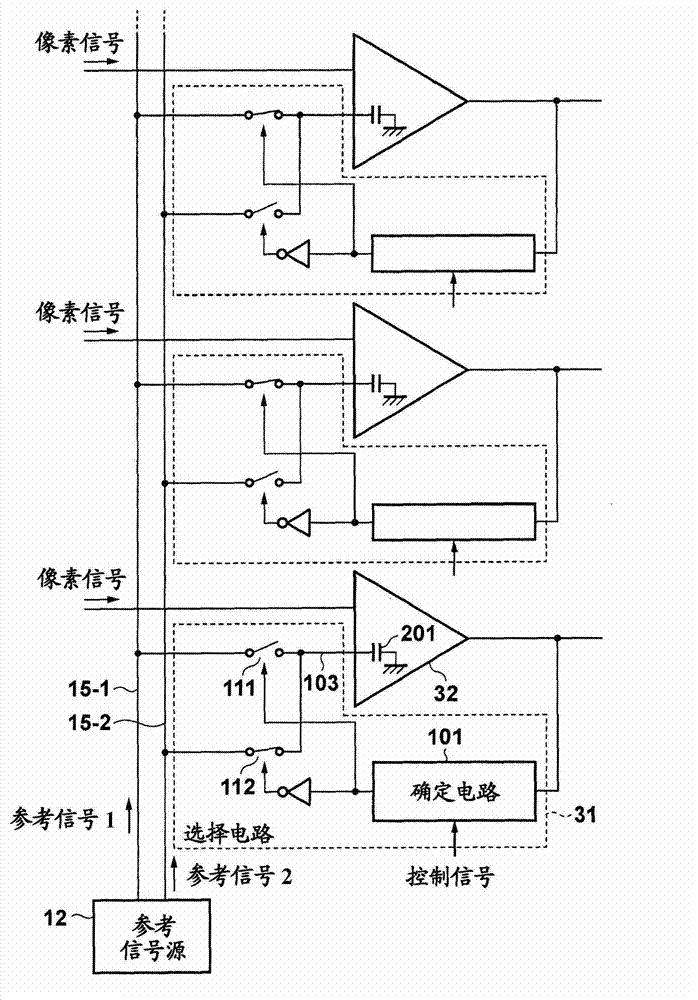
[0072] will refer to Figure 6 The timing chart shown in describes the operation of the selection circuit 31 according to the second embodiment.

[0073] To input the reference signal 1 to the comparator 32 , the selection circuit 31 closes the switch 111 and opens the switch 114 , thereby selectively connecting the reference signal line 15 - 1 to the reference signal connection node 103 . At the same time, the selection circuit 31 opens the switch 112 and closes the switch 113, thereby selectively connecting the capacitor 102 to the reference signal line 15-2. At this time, the pixel outputs a reset signal. During the N conversion period, ...

no. 3 example

[0080] A solid-state image sensing device and an A / D conversion method therefor according to a third embodiment of the present invention will be described below. Note that in the third embodiment, the same components as those in the first and second embodiments have the same reference numerals, and a detailed description thereof will be omitted.

[0081] will refer to Figure 7 The timing chart shown in describes the operation of the selection circuit 31 according to the third embodiment.

[0082] To input the reference signal 1 to the comparator 32 , the selection circuit 31 closes the switch 111 and opens the switch 114 , thereby selectively connecting the reference signal line 15 - 1 to the reference signal connection node 103 . At the same time, the selection circuit 31 opens the switch 112 and closes the switch 113, thereby selectively connecting the capacitor 102 to the reference signal line 15-2. At this time, the pixel outputs a reset signal. During the N conversion...


PUM


Abstract

An image sensor comprises plural sets of a unit pixel outputting a pixel signal based on an electric charge generated through photoelectric conversion and a conversion unit converting the pixel signal into a digital signal. A reference signal source generates reference signals and supplies the generated reference signals to the conversion unit through signal lines. The conversion unit of each set comprises a comparator which compares the level of the reference signal with that of the pixel signal, a count circuit which counts a clock based on the comparison processing, a selection circuit which selects, among the signal lines, a signal line to be selectively connected to the input of the comparator, and a switch which selectively connects the selected signal line to the input of the comparator, and selectively connects a load to an unselected one of the signal lines.

Description

technical field [0001] The present invention relates to solid-state image sensing devices, and more particularly to solid-state image sensing devices including an analog-to-digital conversion unit. Background technique [0002] A CMOS image sensor including an A / D converter (hereinafter will be referred to as “column ADC”) for performing analog-to-digital (A / D) conversion for each column of unit pixels arranged in a matrix topology (topology) is used as a solid-state image sensing device. As an A / D conversion method, a plurality of comparators are used to respectively compare pixel signals with reference signals having different rates of change with respect to time, thereby performing A / D conversion based on the comparison time (see Japanese Patent Laid-Open No.2007-281987 (Document 1)). [0003] Further, there are provided selecting a reference signal suitable for a pixel signal among a plurality of reference signals each having a ramp voltage (ramp voltage) based on a pi...

Claims


Application Information

Patent Timeline
Patent Type & Authority Applications(China)
IPC IPC(8): H04N5/359H04N5/378H04N5/374H04N5/3745
CPCH01L27/14601H04N5/378H03M1/123H03M1/186H03M1/56H04N25/75
Inventor 池田泰二桥本诚二武藤隆松野靖司吉田大介
Owner CANON KK
Why Eureka
Try Eureka