Nanowire field-effect device with multiple gates

A technology of nanowires and devices, which is applied in the field of semiconductor devices and their manufacturing, and can solve problems such as related difficulties

Inactive Publication Date: 2013-08-21
IBM CORP
View PDF3 Cites 6 Cited by
  • Summary
  • Abstract
  • Description
  • Claims
  • Application Information

AI Technical Summary

Problems solved by technology

For example, when the tunnel FET is based on a vertical nanowire process, another challenge will be experienced in creating a steep tunnel junction at the base of the nanowire
Additionally, in some materials, chemical doping of both polarities can be challenging, for example due to difficulties associated with incorporation of the desired doped atoms during growth.
[0010] See now Lee et al., Applied Physics Letters, Vol. 85, pp. 145-147, 2004, reporting that electrostatic doping can mitigate some of the disadvantages associated with impurity doping, especially with temperature-constrained materials (such as III-V systems) related doping, and in which sufficiently activated dopants of one or both polarities are achieved by impurity doping and / or other previously proposed methods with Si The situation is challenging

Method used


Image

  • Nanowire field-effect device with multiple gates
  • Nanowire field-effect device with multiple gates
  • Nanowire field-effect device with multiple gates

Examples


Embodiment Construction

[0028] In the specification, the same reference numerals or signs are used to denote the same parts and the like.

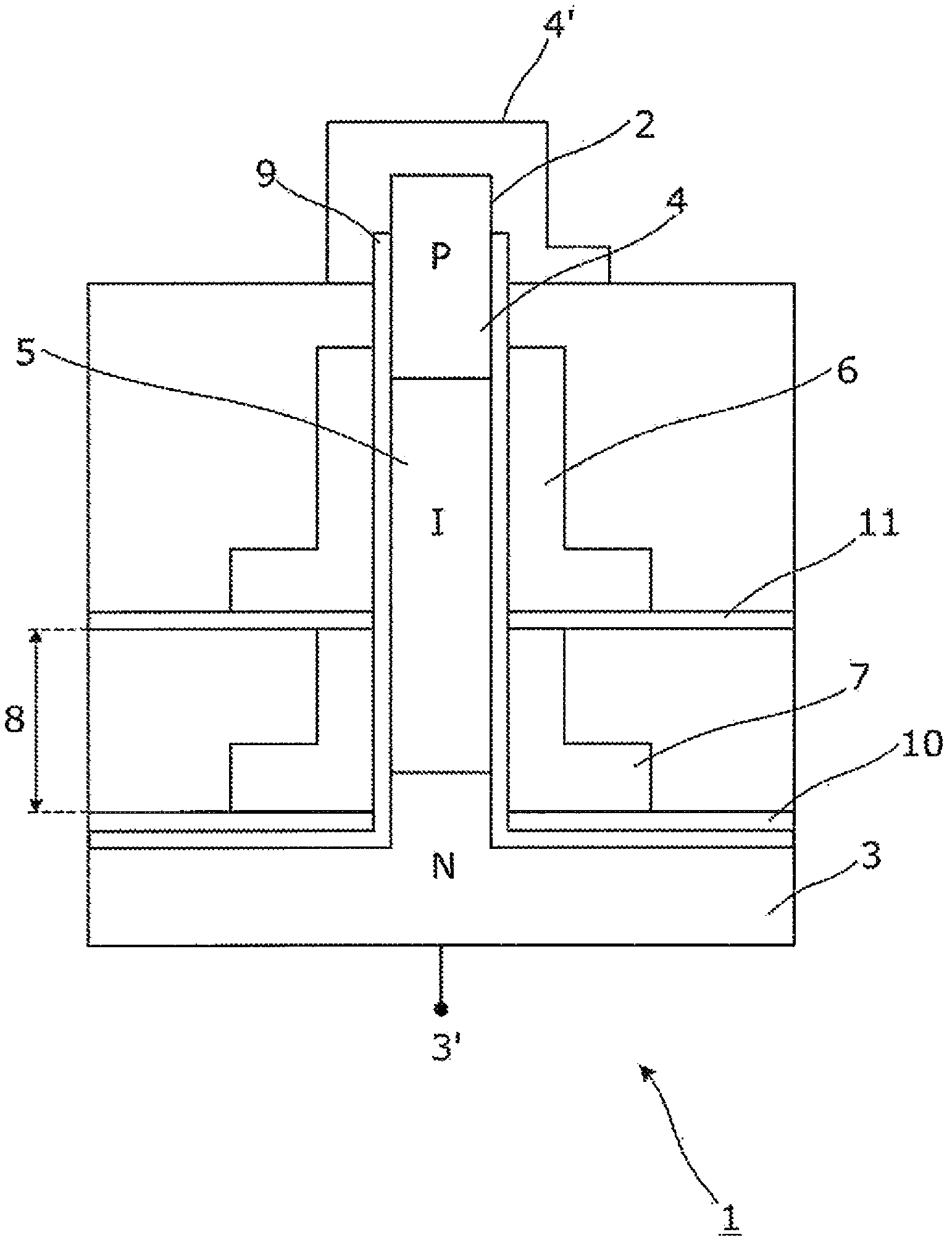
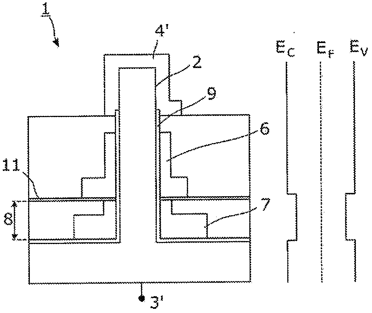
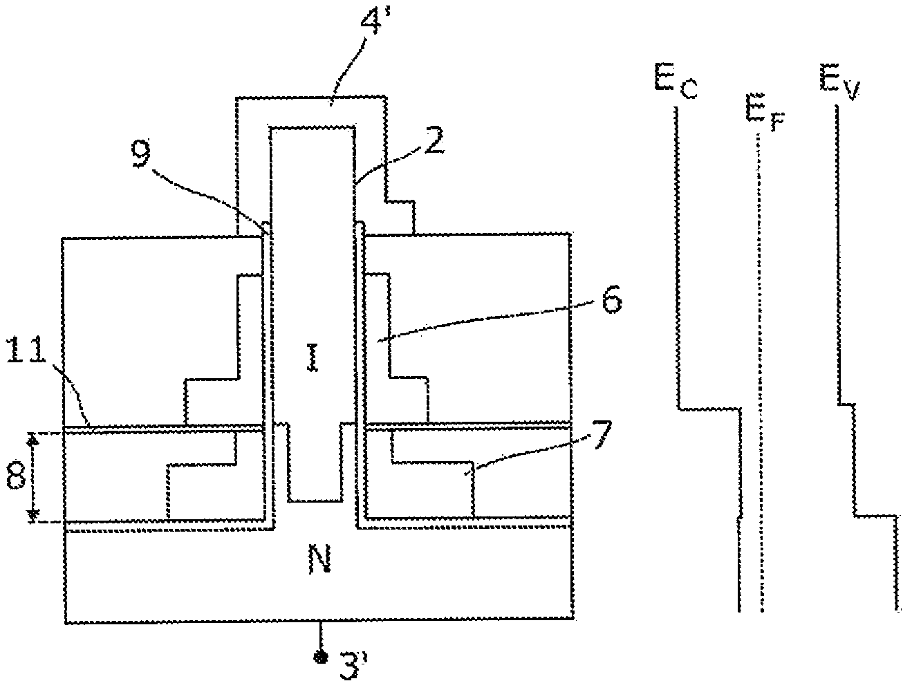
[0029] Refer now figure 1 This figure schematically illustrates an embodiment of the device aspect according to the present invention.

[0030] As from figure 1 It can be seen that the embodiment of the present invention includes a tunnel FET1 that can be implemented by nanowires 2. In this specific example of the embodiment of the invention, the nanowire 2 is aligned substantially vertically and the nanowire 2 is grown / etched from the intrinsic semiconductor substrate. The nanowire 2 is configured to have at least three distinct regions: at least one source region 3 including a corresponding source semiconductor material, at least one drain region 4 including a corresponding drain semiconductor material, and disposed in the source region 3 and the drain region. Between the pole regions 4 includes at least one channel region 5 corresponding to the channel semicondu...


PUM


Abstract

The present invention relates to a semiconductor device (1) comprising: at least a nanowire (2) configured to comprise: at least a source region (3) comprising a corresponding source semiconductor material, at least a drain region (4) comprising a corresponding drain semiconductor material and at least a channel region (5) comprising a corresponding channel semiconductor material, the channel region (5) being arranged between the source region (3) and the drain region (4), at least a gate electrode (6) that is arranged relative to the nanowire (2) to circumferentially surround at least a part of the channel region (5), and at least a strain gate (7) that is arranged relative to the nanowire (2) to circumferentially surround at least a part of a segment of the nanowire (2), the strain gate (7) being configured to apply a strain to the nanowire segment (8), thereby to facilitate at least an alteration of the energy bands corresponding to the source region (3) relative to the energy bands corresponding to the channel region (5).

Description

Technical field [0001] The invention relates to a semiconductor device and a manufacturing method thereof. Background technique [0002] Tunnel field effect transistors (FETs) can be used in several applications including high-speed switching and logic circuits. Unlike the case of other types of FETs, the inverse subthreshold slope of the tunnel FET is not limited to 60 mV / dec at room temperature as determined by the Boltzmann tailing of Fermi statistics. Therefore, the tunnel FET can potentially have a faster turn-on than the previously proposed device, that is, the bias range used to facilitate the transition from the "on" conductive state to the "off" non-conductive state is smaller than the previously proposed device It is possible to reduce both the threshold value and the operating voltage without corresponding degradation of device performance. This makes tunnel FETs particularly suitable for applications where reduced power consumption is desired. [0003] Until recently...

Claims


Application Information

Patent Timeline
Patent Type & Authority Applications(China)
IPC IPC(8): H01L29/10H01L29/423H01L29/775H01L29/06H01L29/78B82Y40/00B82Y10/00H01L29/739
CPCB82Y10/00B82Y40/00H01L29/0676H01L29/068H01L29/1054H01L29/4232H01L29/7391H01L29/775H01L29/66439
Inventor S·F·卡格K·E·莫塞伦德
Owner IBM CORP
Why Eureka
Try Eureka