TFT (thin film transistor) array substrate, and production method thereof and display device

An array substrate and substrate technology, applied in the field of TFT array substrates, TFT array substrate manufacturing methods and display devices, can solve problems such as difficulty in increasing production capacity, achieve the effects of increasing production capacity, avoiding the photoelectric effect, and saving the use of metal materials

Active Publication Date: 2013-08-28
XIAMEN TIANMA MICRO ELECTRONICS
View PDF6 Cites 30 Cited by
  • Summary
  • Abstract
  • Description
  • Claims
  • Application Information

AI Technical Summary

Problems solved by technology

[0018] The embodiment of the present invention provides a TFT array substrate, a manufacturing method of the TFT array substrate, and a display device, to solve the problem that in order to prevent the photoelectric effect from affecting the stability of the TFT s

Method used


Image

  • TFT (thin film transistor) array substrate, and production method thereof and display device
  • TFT (thin film transistor) array substrate, and production method thereof and display device
  • TFT (thin film transistor) array substrate, and production method thereof and display device

Examples


Embodiment 1

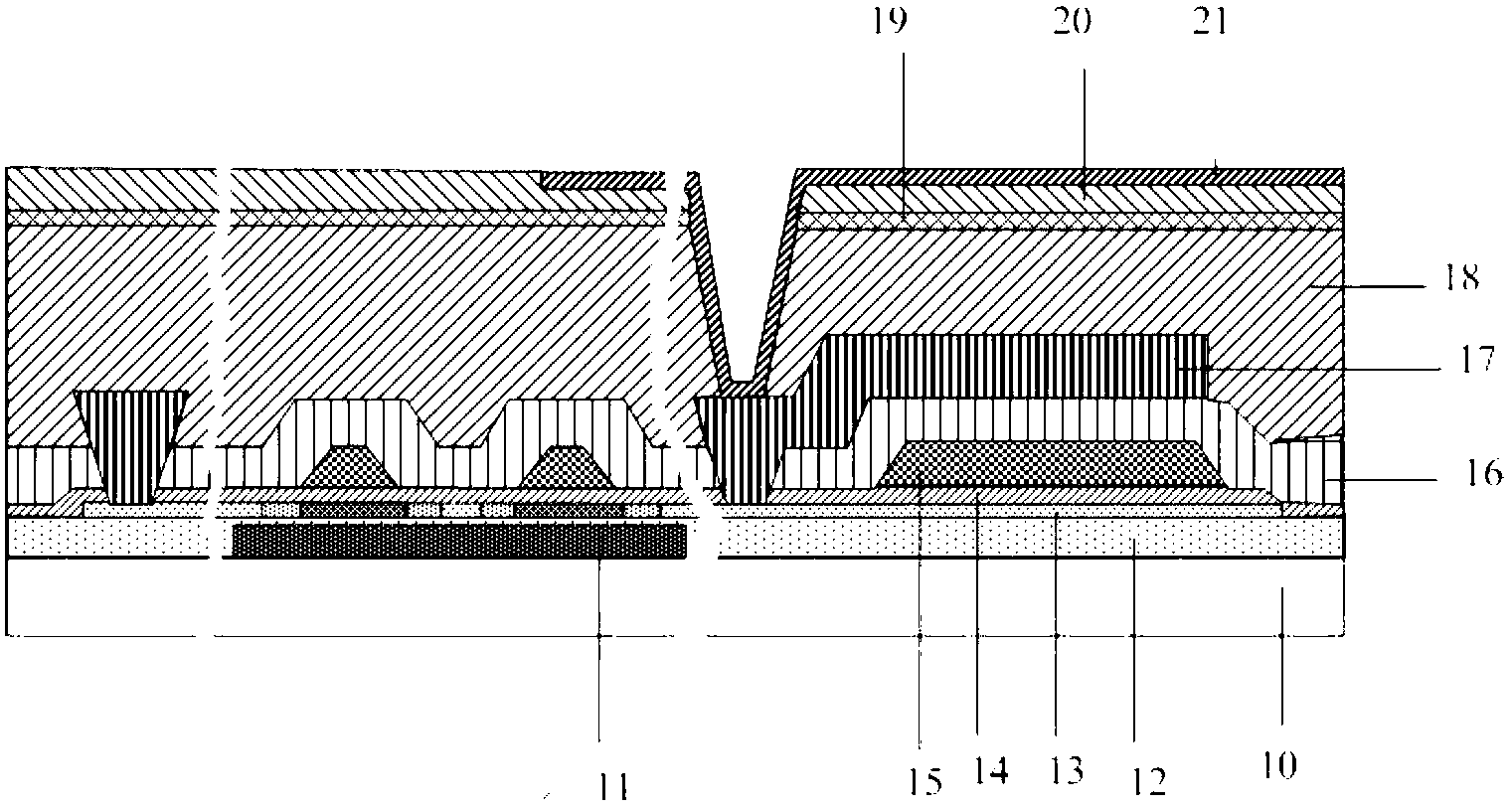
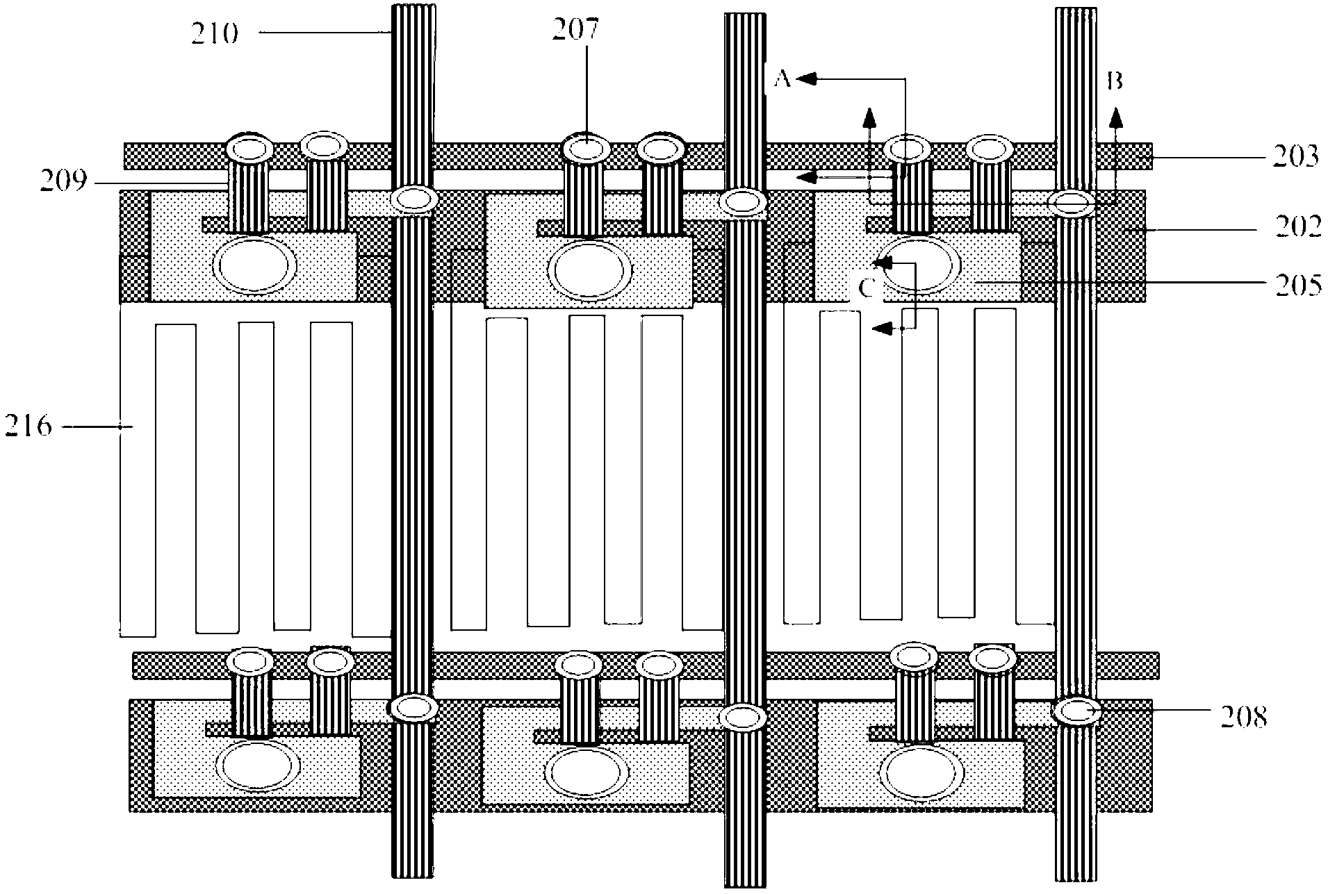
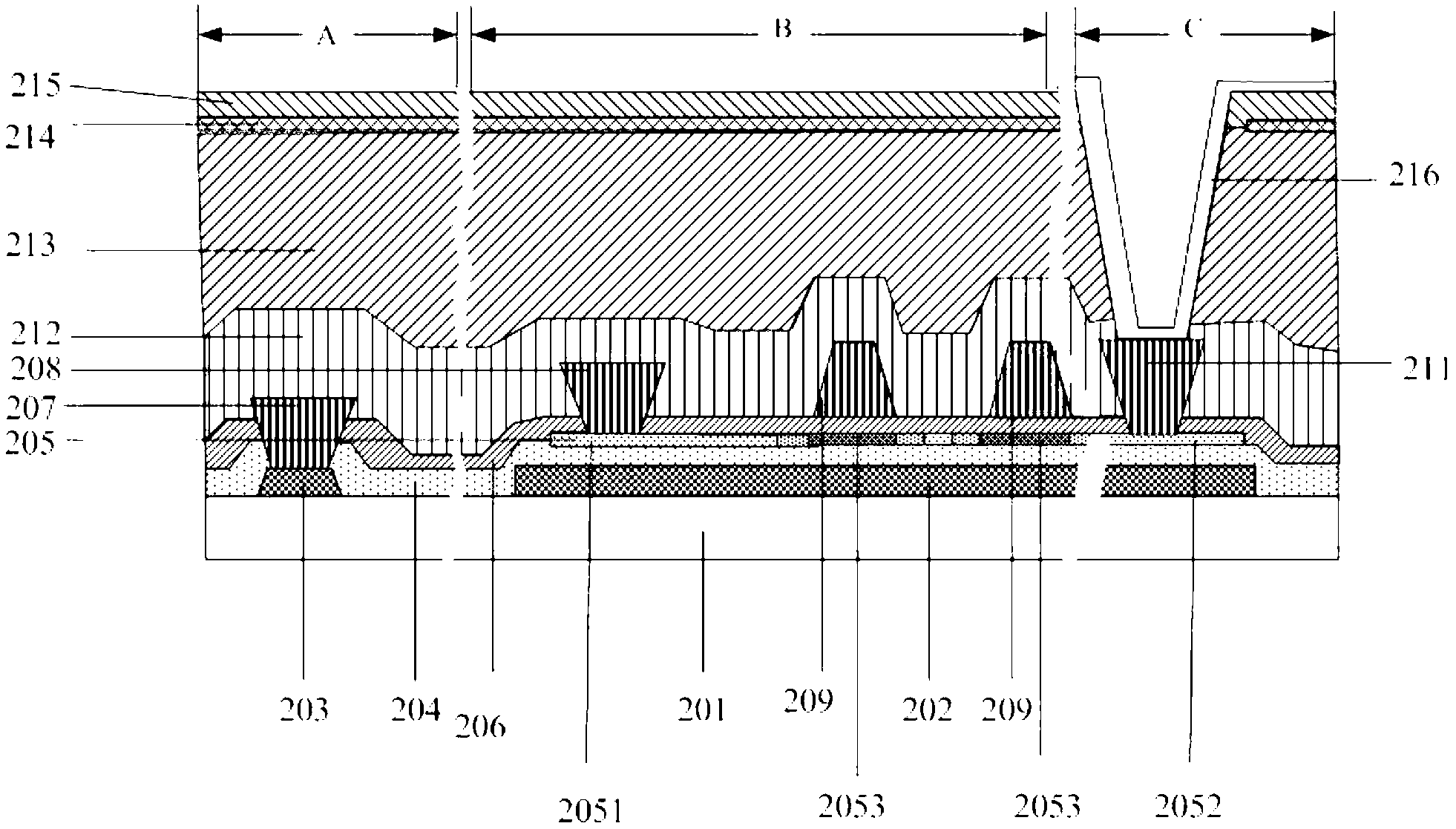
[0095] The first embodiment of the present invention takes the FFS mode as an example to illustrate the structure of the TFT array substrate in the lateral electric field mode. figure 2 with 3 As shown, they are respectively a schematic plan view and a cross-sectional structure view of an FFS mode TFT array substrate provided by the first embodiment of the present invention, in which, figure 2 The three parts A, B, and C correspond to image 3 In parts A, B, and C, the TFT array substrate includes:

[0096] The substrate 201, the common electrode line 202, the gate line 203, the insulating buffer layer 204, the active layer 205, the gate insulating layer 206, the gate lead 207, the source 208, the gate 209 and the data line 210; among them:

[0097] The common electrode line 202 and the gate line 203 extend along a first direction and are formed on the substrate;

[0098] The insulating buffer layer 204 is formed on the common electrode line 202 and the gate line 203;

[0099] The ac...

Embodiment 2

[0128] The second embodiment of the present invention describes the manufacturing method of the FFS mode TFT array substrate in the first embodiment. Such as Figure 5 As shown, it is a schematic flow chart of the manufacturing method of the TFT array substrate according to the second embodiment of the present invention, including the following steps:

[0129] Step 101: At Figure 6a The first metal layer is deposited on the substrate shown, and formed by a mask process such as Figure 6b As shown in the common electrode lines and gate lines extending in the first direction, the first metal layer is opaque.

[0130] Step 102: Deposit an insulating buffer layer and an amorphous silicon layer sequentially on the substrate on which the common electrode line and the gate line are formed, and form an active layer on the amorphous silicon layer through an excimer laser thermal annealing process, a mask process, and a doping process The active layer includes a source region, a drain regio...

Embodiment 3

[0168] The third embodiment of the present invention uses the TN mode as an example to illustrate the structure of the TFT array substrate in the lateral electric field mode. figure 2 with Picture 9 As shown, they are respectively a schematic plan view and a schematic cross-sectional structure view of a TN mode TFT array substrate provided in the third embodiment of the present invention, in which, figure 2 The three parts A, B, and C correspond to Picture 9 In parts A, B, and C, the TFT array substrate includes:

[0169] The substrate 201, the common electrode line 202, the gate line 203, the insulating buffer layer 204, the active layer 205, the gate insulating layer 206, the gate lead 207, the source electrode 208, the gate 209 and the data line 210; among them:

[0170] The common electrode line 202 and the gate line 203 extend along a first direction and are formed on the substrate;

[0171] The insulating buffer layer 204 is formed on the common electrode line 202 and the ga...


PUM


Abstract

The invention provides a TFT (thin film transistor) array substrate, and a production method thereof and a display device. The TFT array substrate mainly comprises a substrate, a common electrode wire, a grid wire, an insulation buffering layer, an active layer, a grid electrode insulation layer, a grid lead, a source electrode, a grid electrode and a data wire wherein the common electrode wire and the grid wire are formed on the substrate and extend along a first direction; the insulation buffering layer is formed on the common electrode wire and the grid wire; the active layer is formed on the insulation buffering layer; and the grid electrode insulation layer is formed on the active layer, and the grid lead, the source electrode, the grid electrode and the data wire are formed on the grid electrode insulation layer. Since the common electrode wire is made of a nontransparent metal, and a ditch area is arranged right above the common electrode wire, the high-bright backlight can be efficiently shielded by the common electrode wire, so that the photovoltaic effect which is produced under the influence of the high-bright backlight in the ditch area can be avoided. Therefore, according to the scheme provided by the invention, alight shielding layer is not required to be specially arranged, so that one procedure is omitted, the metal material is reduced, and the productivity of the TFT array substrate can be effectively improved.

Description

Technical field [0001] The present invention relates to the field of liquid crystal display technology, in particular to a TFT array substrate, a manufacturing method of the TFT array substrate, and a display device. Background technique [0002] With the evolution of mainstream liquid crystal display screens in the market, the screen resolution of Thin Firm Transistor Liquid Crystal Display (TFT-LCD) has gradually increased. In the case of the same display panel size, the total number of pixels of the panel will increase, which will cause the transmittance of the panel to decrease. However, when the panel brightness is unchanged, as the panel transmittance decreases, it is bound to use a higher brightness backlight To meet the demand for constant brightness, high-brightness backlight will increase the photoelectric effect, which will affect the off-state leakage current of the TFT, which means that the stability of the TFT switch is reduced. [0003] In order to improve the stabi...

Claims


Application Information

Patent Timeline
IPC IPC(8): H01L27/12H01L21/77G02F1/1362G02F1/1368
Inventor 林嘉民李俊谊彭涛
Owner XIAMEN TIANMA MICRO ELECTRONICS
Why Eureka
Try Eureka