
Capacity touch panel employing copper-plated conductive substrate

A technology of capacitive touch screen and conductive substrate, applied in the direction of electrical digital data processing, input/output process of data processing, instruments, etc., can solve the problem of low production yield and efficiency, increase the difficulty of process requirements, and reduce production costs, etc. problems, to achieve production yield and increase production efficiency, to meet the design requirements of narrow bezel products, and to achieve the effect of small wiring space requirements

Inactive Publication Date: 2013-09-04
GUANGDONG GREEN PRECISION COMPONENTS CO LTD
View PDF9 Cites 12 Cited by
  • Summary
  • Abstract
  • Description
  • Claims
  • Application Information

AI Technical Summary

Problems solved by technology

[0006] 1. The produced line width and line spacing are relatively large, and the required wiring frame is relatively large, which increases the difficulty of process requirements and increases the production cost;
[0007] 2. The process requirements are relatively complicated, and the production excellent rate and efficiency are low, which is not conducive to the company's better reduction of production costs
In its invention, complex metal bridges need to be built, the process flow is relatively complicated, and the production yield and efficiency are low

Method used


Image

  • Capacity touch panel employing copper-plated conductive substrate
  • Capacity touch panel employing copper-plated conductive substrate
  • Capacity touch panel employing copper-plated conductive substrate

Examples


Embodiment Construction

[0023] The capacitive touch screen with a copper-plated conductive substrate provided by the invention can reduce raw material and processing costs, improve production efficiency, and thus increase production capacity.

[0024] The technical solution in the present invention will be clearly and completely described below in conjunction with the accompanying drawings in the present invention. Obviously, what is described is only a part of the embodiments of the present invention, not all the embodiments. Based on the embodiments of the present invention, all other embodiments obtained by persons of ordinary skill in the art without creative efforts fall within the protection scope of the present invention.

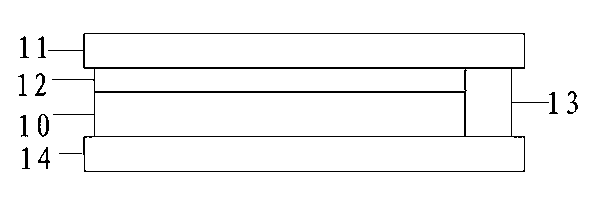
[0025] see image 3 It is a schematic structural diagram of a capacitive touch screen with a copper-plated conductive substrate provided by the present invention. Including liquid crystal module LCM 1, sensor 2, cover plate Cover Lens 3, optical double-sided adhesive tape ...


PUM


Abstract

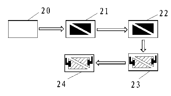
The invention provides a capacity touch panel employing a copper-plated conductive substrate, and belongs to the field of capacity touch panels. The capacity touch panel comprises a cover lens arranged outmost, a sensor bonded with the cover lens and an LCM (liquid crystal module) attached on the inner side of the capacity touch panel. The sensor is manufactured by processes of firstly, sputtering copper foil on the conductive substrate through a film coating process; secondly, forming a copper film signal line graph on the conductive substrate by performing operations of exposure, development and etching on a copper plated film by the aid of a dry film photoresist; thirdly, forming a transparent conductive film graph with the copper film signal line graph on the conductive substrate with the copper film signal line graph by operations of exposure, development and etching; and fourthly, cutting to obtain the sensor. The capacity touch panel employing the copper plated conductive substrate has the advantages that raw materials and processing cost can be reduced, production efficiency can be increased, and productivity can be improved.

Description

technical field [0001] The invention relates to the field of capacitive touch screens, in particular to a capacitive touch screen using a copper-plated conductive substrate. Background technique [0002] Touch screens are composite touch screens used in electronic products such as mobile phones, e-books, and digital cameras, among which capacitive touch screens are the most commonly used type of touch screens. [0003] The capacitive touch screen uses the current induction of the human body to work. The capacitive touch screen is usually a four-layer composite glass screen. The inner surface and interlayer of the glass screen are each coated with a layer of ITO (coated conductive glass), and the outermost layer is A thin layer of silica glass protective layer, ITO coating as the working surface, four electrodes are drawn from the four corners, and the inner layer of ITO is the shielding layer to ensure a good working environment; when the user's finger touches the capacitive...

Claims


Application Information

Patent Timeline
IPC IPC(8): G06F3/044
Inventor 吴宝玉方维祥
Owner GUANGDONG GREEN PRECISION COMPONENTS CO LTD
Learn More