

Manufacturing method for gate dielectric layer and manufacturing method for transistor
A manufacturing method and gate dielectric layer technology, which are applied in the manufacture of gate dielectric layers and the field of transistor manufacturing, can solve the problems of poor interface characteristics, affecting the interface characteristics of the interface layer and high-k gate dielectric layer, and poor quality of the interface layer. To achieve the effect of improving the interface characteristics
- Summary
- Abstract
- Description
- Claims
- Application Information
AI Technical Summary
Problems solved by technology
Method used
Image


Examples
Embodiment 1
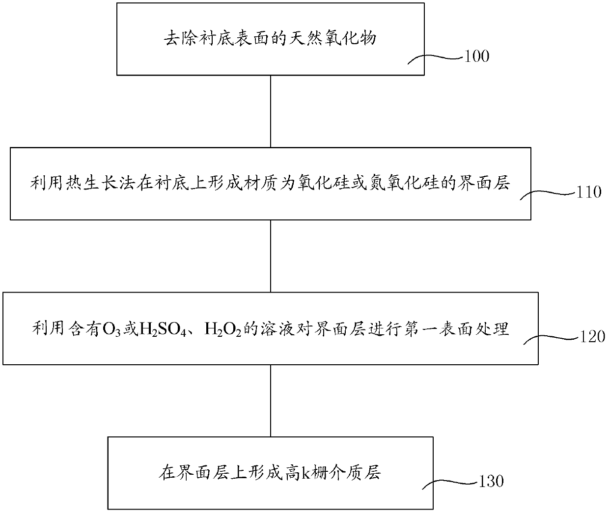
[0047] figure 1 It is the fabrication flowchart of the gate dielectric layer in Embodiment 1 of the gate dielectric layer fabrication method of the present invention, as shown in figure 1 As shown, the method includes:
[0048] Step S100: removing natural oxides on the surface of the substrate.
[0049] Step S110: forming an interface layer made of silicon oxide or silicon oxynitride on the substrate by thermal growth method.
[0050] Step S120: Using the 3 or contain H 2 SO 4 、H 2 o 2 The aqueous solution of the interface layer is subjected to the first surface treatment.
[0051] Step S130: forming a high-k gate dielectric layer on the interface layer.
[0052] Combine below figure 1 The method for fabricating the gate dielectric layer of the present invention will be described in detail.
[0053] execute first figure 1 Step S100 in: removing the native oxide on the surface of the substrate.
[0054] When the substrate is exposed to air, the surface of the substr...
Embodiment 2
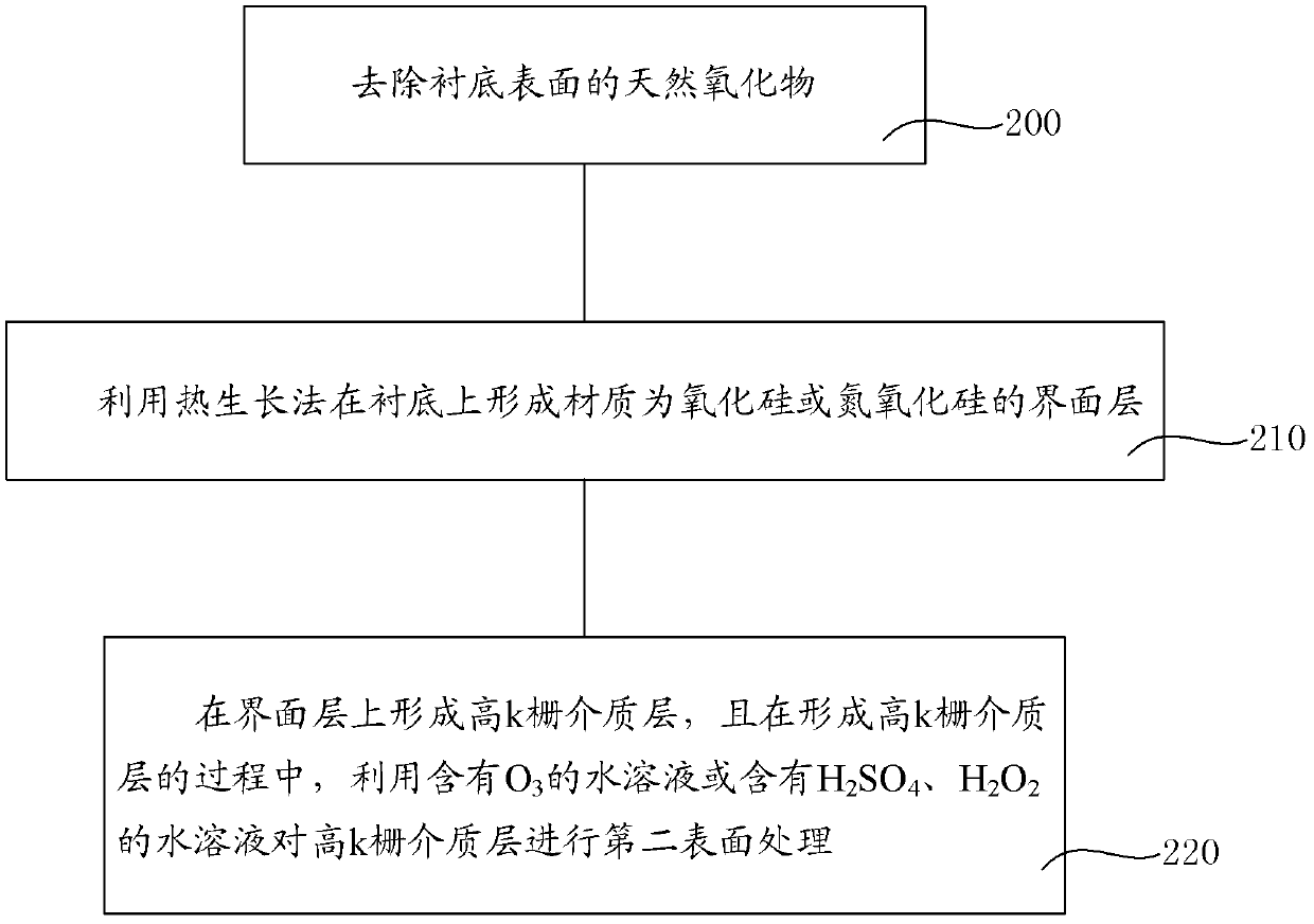
[0070] figure 2 It is the fabrication flowchart of the gate dielectric layer in Embodiment 2 of the gate dielectric layer fabrication method of the present invention, as shown in figure 2 As shown, the method includes:
[0071] Step S200: removing natural oxides on the surface of the substrate.
[0072] Step S210: forming an interface layer made of silicon oxide or silicon oxynitride on the substrate by thermal growth method.
[0073] Step S220: forming a high-k gate dielectric layer on the interface layer, and in the process of forming the high-k gate dielectric layer, using 3 or contain H 2 SO 4 、H 2 o 2 The aqueous solution of the high-k gate dielectric layer is subjected to the second surface treatment.
[0074] Combine below figure 2 The method for fabricating the gate dielectric layer of the present invention will be described in detail.
[0075] execute first figure 2 Step S200 in: removing the natural oxide on the surface of the substrate.
[0076] When ...
Embodiment 3
[0094] image 3 It is the fabrication flowchart of the gate dielectric layer in Embodiment 3 of the gate dielectric layer fabrication method of the present invention, as shown in image 3 As shown, the method includes:
[0095] Step S300: removing natural oxides on the surface of the substrate.
[0096] Step S310: forming an interface layer made of silicon oxide or silicon oxynitride on the substrate by thermal growth method.
[0097] Step S320: Using the 3 or contain H 2 SO 4 、H 2 o 2 The aqueous solution of the interface layer is subjected to the first surface treatment.
[0098] Step S330: forming a high-k gate dielectric layer on the interface layer, and in the process of forming the high-k gate dielectric layer, using 3 or contain H 2 SO 4 、H 2 o 2 The aqueous solution of the high-k gate dielectric layer is subjected to the second surface treatment.
[0099] Combine below image 3 The method for fabricating the gate dielectric layer of the present invention ...
PUM
 Abstract
Description
Claims
Application Information