Manufacturing method of tsv adapter board and tsv adapter board

A manufacturing method and a technology for an adapter board, which are applied in the field of microelectronics, can solve the problems of reducing the reliability of the electrical connection of the TSV adapter board, high cost of the TSV adapter board, and easy to reduce the conductivity of bumps, etc. The effect of improving reliability and reducing production costs

Active Publication Date: 2016-02-10
BEIJING NAURA MICROELECTRONICS EQUIP CO LTD
View PDF3 Cites 0 Cited by
  • Summary
  • Abstract
  • Description
  • Claims
  • Application Information

AI Technical Summary

Problems solved by technology

[0006] It can be seen from the above that the current process of making bumps requires two photolithography processes, which makes the cost of the TSV adapter board relatively high
Moreover, the photoresist is an organic substance, which has a negative impact on the electroplating process, and easily reduces the conductivity of the bumps, thereby reducing the reliability of the electrical connection of the TSV adapter board

Method used


Image

  • Manufacturing method of tsv adapter board and tsv adapter board
  • Manufacturing method of tsv adapter board and tsv adapter board
  • Manufacturing method of tsv adapter board and tsv adapter board

Examples


Embodiment Construction

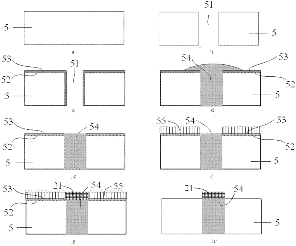
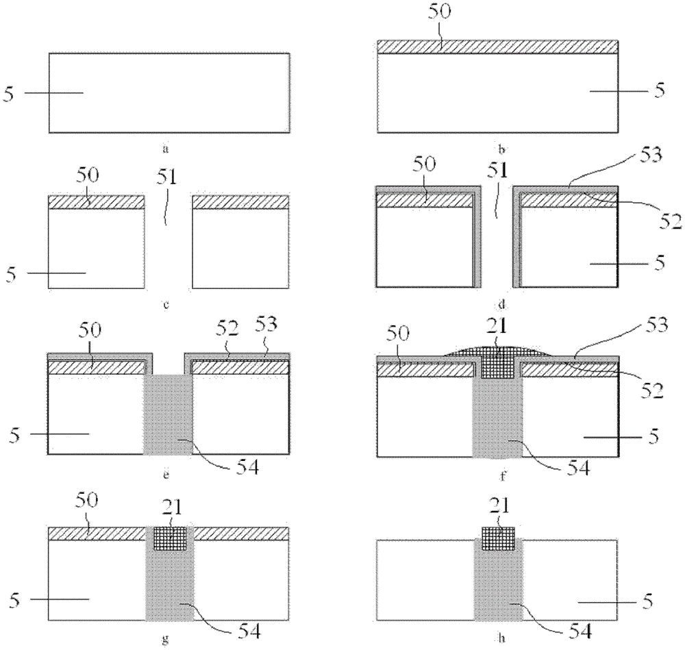
[0036] In order to enable those skilled in the art to better understand the technical solution of the present invention, the manufacturing method of the TSV adapter plate and the TSV adapter plate provided by the present invention will be described in detail below with reference to the accompanying drawings.

[0037] image 3 a- image 3 h is a schematic diagram of the manufacturing process of the TSV adapter plate provided by the embodiment of the present invention. Figure 4 It is a flow chart of the manufacturing process of the TSV adapter board according to the embodiment of the present invention. Please also refer to image 3 a- image 3 h and Figure 4 , the manufacturing method of the TSV adapter board provided in this embodiment includes the following steps:

[0038] Step s10, obtaining a substrate.

[0039] The substrate 5 of the present embodiment is a silicon wafer, such as image 3 as shown in a. It is not difficult to understand that the substrate 5 can al...


PUM


Abstract

The invention provides a manufacturing method of a TSV adapter plate and a TSV adapter plate. The method comprises a step of obtaining a substrate and manufacturing a sacrificial layer on the surface of the substrate, a step of manufacturing a through hole in the substrate through the photoetching and etching technology, wherein the through hole penetrates through the substrate and the sacrificial layer, a step of manufacturing an electric conduction pillar and a protruding point at the through hole position, wherein the protruding point is located at the top end of the electric conduction pillar, and the top of the protruding point is higher than the upper surface of the sacrificial layer, a step of removing materials on the upper surface of the sacrificial layer, and a step of removing the sacrificial layer on the upper surface of the substrate, so that the protruding point is obtained at the through hole position. According to the manufacturing method, working procedures are simplified, so that production cost is reduced, production efficiency is improved, and the reliability of the TSV adapter plate is improved.

Description

technical field [0001] The invention belongs to the technical field of microelectronics, and relates to a manufacturing method of a TSV adapter plate and the TSV adapter plate. Background technique [0002] With the continuous progress of microelectronics technology, it is no longer possible to meet the actual needs only by integrating more devices on a single chip to improve the performance of the chip. Therefore, stacked chip packaging technology has gradually become the mainstream of technology development. Stacked chip packaging technology is a packaging technology that stacks multiple chips vertically in the same package without changing the size of the package. Among them, the through-silicon via (Through Sivia, TSV) adapter board is a connection board to realize the interconnection of upper and lower chips. The TSV adapter board mainly includes three parts: TSV through hole, transfer circuit and bump, which can not only reduce the The length of the interconnection l...

Claims


Application Information

Patent Timeline
Patent Type & Authority Patents(China)
IPC IPC(8): H01L21/48H01L23/538
CPCH01L2224/16225H01L2924/15311
Inventor 边国栋
Owner BEIJING NAURA MICROELECTRONICS EQUIP CO LTD
Why Eureka
Try Eureka