Array substrate row driving circuit

A technology of array substrate row and drive circuit, applied in static memory, instrument, static indicator, etc., can solve the problems of large leakage current of thin film transistor, difficult to control accurately, and disadvantageous to display quality of liquid crystal display, etc., and achieve the effect of improving display quality

Active Publication Date: 2013-09-18
TCL CHINA STAR OPTOELECTRONICS TECH CO LTD
View PDF8 Cites 60 Cited by
  • Summary
  • Abstract
  • Description
  • Claims
  • Application Information

AI Technical Summary

Problems solved by technology

like figure 2 As shown, it is the I-V curve (current-voltage curve) of the characteristics of the thin film transistor. It can be seen from this figure that V gs When it is 0V, the current flowing through the thin film transist

Method used


Image

  • Array substrate row driving circuit
  • Array substrate row driving circuit
  • Array substrate row driving circuit

Examples


Embodiment Construction

[0032] In order to further illustrate the technical means adopted by the present invention and its effects, the following describes in detail in conjunction with preferred embodiments of the present invention and accompanying drawings.

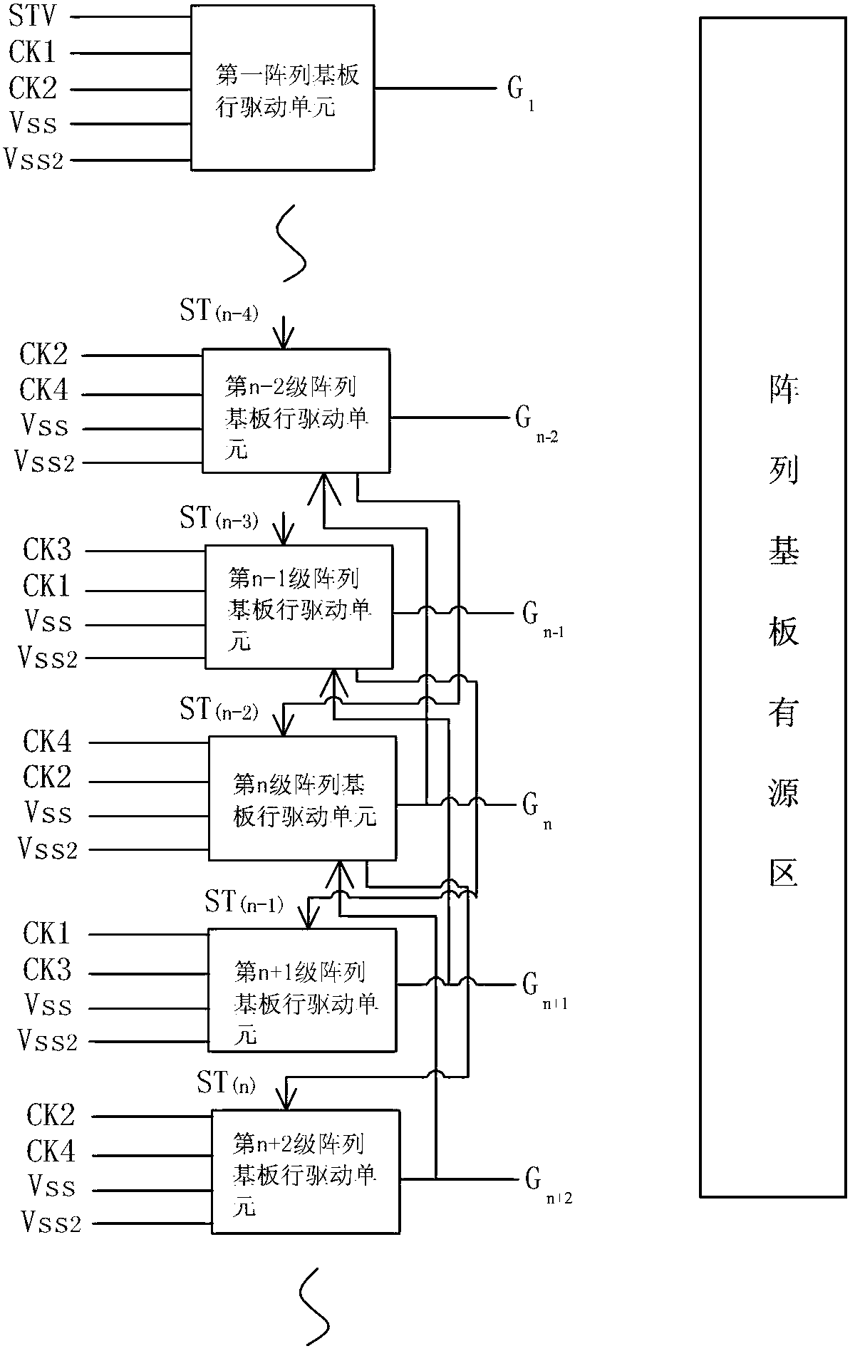
[0033] see Figures 3 to 5 , the present invention provides an array substrate row driving circuit, including several cascaded multi-level array substrate row driving units, wherein the nth-level array substrate row driving unit of the array substrate row driving circuit has an n-2th level Signal input terminal (ST n-2 ) 21. The n+2 level signal input terminal (G n+2 ) 22, the first clock signal input terminal 23, the clock signal second input terminal 24, the first low level input terminal 25, the second low level input terminal 26, the first output terminal (G n ) 27 and the second output terminal (ST n ) 28.

[0034] The connection of the row driving units of the cascaded array substrates has the same structure, except for the first two...


PUM


Abstract

The invention provides an array substrate row driving circuit. The driving circuit comprises multiple array substrate row driving units, wherein an n-level array substrate row driving unit of the array substrate row driving circuit comprises an n-2 level signal input end (21), an n+2 level signal input end (22), a clock signal first input end (23), a clock signal second input end (24), a first low electric level input end (25), a second low electric level input end (26), a first output end (27), a second output end (28), a pull-up driving unit (32), a pull-up unit (34) and first to third pull-down units (36, 37 and 38). As a second low electric level signal is added, and the second low electric level is utilized to lower a voltage difference Vgs between a gate and a source of the first output end thin-film transistor, relatively low leakage current of the thin-film transistor is obtained, and precise control is achieved.

Description

technical field [0001] The present invention relates to the field of display technology, in particular to an array substrate row driving circuit. Background technique [0002] Liquid crystal displays have many advantages such as thin body, power saving, and no radiation, and have been widely used. Most of the liquid crystal displays currently on the market are backlight liquid crystal displays, which include a liquid crystal panel and a backlight module. The working principle of the liquid crystal panel is to place liquid crystal molecules between two parallel glass substrates, and apply a driving voltage on the two glass substrates to control the rotation direction of the liquid crystal molecules, so as to refract the light from the backlight module to produce a picture. [0003] In recent years, the development of liquid crystal displays has shown a trend of high integration and low cost. One of the very important technologies is the mass production of Gate Drive on Arra...

Claims


Application Information

Patent Timeline
IPC IPC(8): G09G3/36
CPCG09G3/3674G09G3/20G09G2310/0267G09G2310/0286G11C19/28
Inventor 曾丽媚林师勤
Owner TCL CHINA STAR OPTOELECTRONICS TECH CO LTD
Why Eureka
Try Eureka