

Preparation method for silica-based gallium arsenide material with high quality and low surface roughness
A silicon-based gallium arsenide, low surface technology, applied in the field of silicon-based gallium arsenide material preparation, can solve the problems of low surface roughness and achieve the effect of low polishing rate
- Summary
- Abstract
- Description
- Claims
- Application Information
AI Technical Summary
Problems solved by technology
Method used
Image

Examples
Embodiment Construction
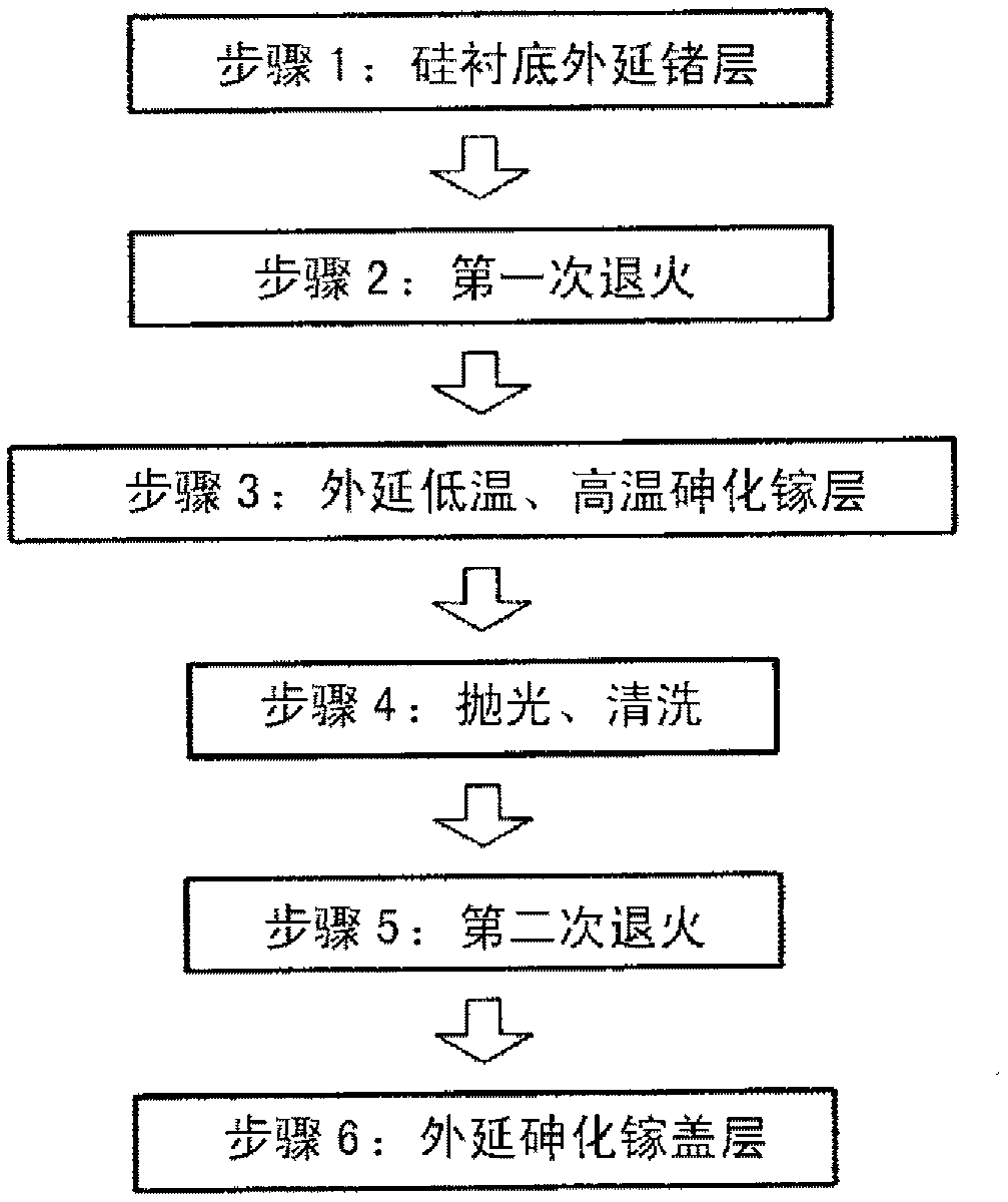
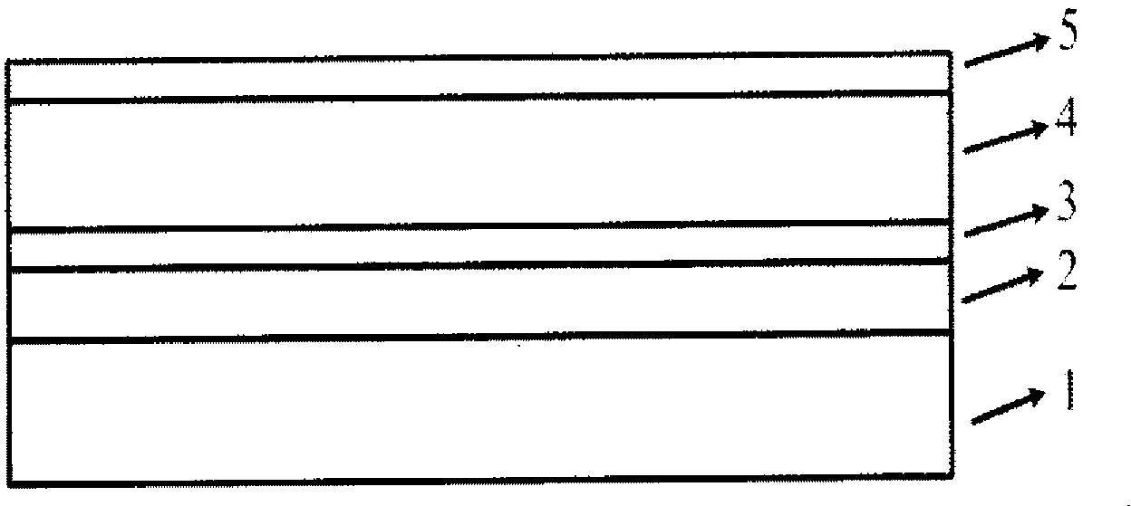
[0021] see figure 1 and figure 2 As shown, the present invention provides a method for preparing a silicon-based gallium arsenide material with high quality and low surface roughness, comprising the following steps:
[0022] Step 1: growing a germanium layer 2 on a silicon substrate 1 . This silicon substrate 1 is the (100) substrate of partial [011] direction 4 °, and size mainly depends on three equipments that need in this method: ultra-low vacuum chemical vapor phase epitaxy (UHVCVD), metal-organic chemical vapor deposition ( MOCVD) and polishing equipment, the size of the epitaxial wafers of the three equipments needs to be consistent, which can be 2 inches to 12 inches, or even larger; the growth of germanium layer 2 adopts UHVCVD, and the low-temperature germanium seed layer and the high-temperature germanium layer are cycled twice. technology, this step is a key step to obtain high-quality gallium arsenide, and the defect density of the germanium layer is required t...
PUM
 Abstract
Description
Claims
Application Information