GaN-based luminous diode chip with current blocking structure and manufacturing method thereof

A technology of light-emitting diodes and current blocking, applied in circuits, electrical components, semiconductor devices, etc., can solve the problems of limited current expansion capacity of ITO electrodes and inability to bond wires, etc., to improve external quantum efficiency, reduce light absorption, and improve light effective effect

Active Publication Date: 2013-09-25
吴江市民福电缆附件厂
View PDF7 Cites 15 Cited by
  • Summary
  • Abstract
  • Description
  • Claims
  • Application Information

AI Technical Summary

Problems solved by technology

But there are still two problems: 1. The current expansion capability of ITO electrodes is limited; 2. It is impossible to weld wires on ITO materials.
[0006] The current blocking structure mentioned above does not emit light in the epitaxial layer directly below the metal electrode, which

Method used


Image

  • GaN-based luminous diode chip with current blocking structure and manufacturing method thereof
  • GaN-based luminous diode chip with current blocking structure and manufacturing method thereof
  • GaN-based luminous diode chip with current blocking structure and manufacturing method thereof

Examples


Embodiment 1

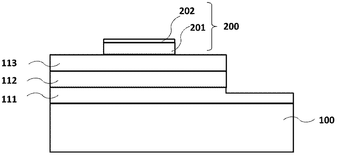
[0036]A GaN-based light-emitting diode chip with a current blocking structure, comprising an epitaxial layer structure, a p-electrode formed on the surface of the p-type GaN of the epitaxial layer structure, and an n-electrode formed on the surface of the n-type GaN of the epitaxial layer structure 400, the p-electrode is composed of an ITO transparent electrode 300 and a metal electrode 200, the metal electrode 200 is composed of upper and lower layers of metal materials, and the metal electrode is located between the ITO transparent electrode and p-type GaN and surrounded by the ITO transparent electrode In the middle, the lower layer 201 of the metal electrode is in Schottky contact with the p-type GaN surface, the metal electrode is in ohmic contact with the ITO transparent electrode, the ITO transparent electrode is in ohmic contact with the p-type GaN surface, and the ITO transparent electrode above the metal electrode is in ohmic contact. A window 301 is partly opened an...

Embodiment 2

[0048] A GaN-based light-emitting diode chip with a current blocking structure, as described in Embodiment 1, the difference is that the material of the upper layer of the metal electrode is chromium with a thickness of 100 nm, and the material of the lower layer of the metal electrode is aluminum with a thickness of 2.5 microns, The ITO transparent electrode part above the metal electrode has two windows and penetrates the upper layer of the metal electrode to expose the lower layer of the metal electrode, and the area of ​​each window is 1 / 3 of the area of ​​the metal electrode. The thickness of the ITO transparent electrode on the p-type GaN surface is 100 nm.

[0049] The n-electrode is different from the metal electrode, it is a Ti / Al electrode made separately, and Ti is located between the Al layer and n-GaN, the thickness of Ti is 100nm, and the thickness of Al is 2 microns.

[0050] The GaN-based light-emitting diode chip with the current blocking structure of this emb...


PUM

PropertyMeasurementUnit
Thicknessaaaaaaaaaa
Thicknessaaaaaaaaaa
Thicknessaaaaaaaaaa

Abstract

The invention relates to a GaN-based luminous diode chip with a current blocking structure and a manufacturing method of the GaN-based luminous diode chip. The GaN-based luminous diode chip comprises an epitaxial layer structure, a p electrode and an n electrode. The p electrode is composed of an ITO transparent electrode and a metal electrode. The metal electrode is located between the ITO transparent electrode and a p-type GaN and is surrounded by the ITO transparent electrode, the lower layer of the metal electrode is contacted with the p-type GaN in a Schottky mode, the metal electrode is contacted with the ITO transparent electrode in an Ohmic mode, the ITO transparent electrode is contacted with the p-type GaN in a Ohmic mode, and a window is formed in part of the ITO transparent electrode on the metal electrode. When the GaN-based luminous diode chip works, a great amount of light obliquely emitted to the lower surface of the metal electrode from the two sides is reflected back to the epitaxial layer layer, therefore, light absorbing amount of the metal electrode is reduced and external quantum efficiency of an LED is improved.

Description

technical field [0001] The invention relates to a GaN-based light-emitting diode chip with a current blocking structure and a manufacturing method thereof, which is applied to making a high-brightness GaN-based light-emitting diode chip. Background technique [0002] Since the 1990s, GaN-based blue LEDs have been widely used as a new type of light source in various fields of social life, such as outdoor display, landscape lighting, and instrument indication. At present, white lighting products based on GaN-based blue LEDs are beginning to be applied in the lighting field. However, a key factor restricting the development of semiconductor lighting is the light efficiency of GaN-based blue LEDs, including internal quantum efficiency and external quantum efficiency. Today, the development of epitaxial technology can increase the internal quantum efficiency to more than 90%, but the external quantum efficiency is very low. [0003] ITO transparent electrode technology plays an...

Claims


Application Information

Patent Timeline
IPC IPC(8): H01L33/14H01L33/40H01L33/00
Inventor 徐化勇沈燕王成新
Owner 吴江市民福电缆附件厂
Why Eureka
Try Eureka