Photoresist reworking etching process

A process and lithography technology, applied in the field of lithography rework etching process, can solve problems such as increasing process complexity, achieve the effect of improving performance and yield, and simplifying process

Active Publication Date: 2013-10-09
SHANGHAI HUALI MICROELECTRONICS CORP
View PDF7 Cites 1 Cited by
  • Summary
  • Abstract
  • Description
  • Claims
  • Application Information

AI Technical Summary

Problems solved by technology

However, although the oxide capping film 15 can well resist the damage to the non-nitrogen bottom anti-reflective film in the wet stripping or dry stripping, it is not compat

Method used


Image

  • Photoresist reworking etching process
  • Photoresist reworking etching process
  • Photoresist reworking etching process

Examples


Embodiment Construction

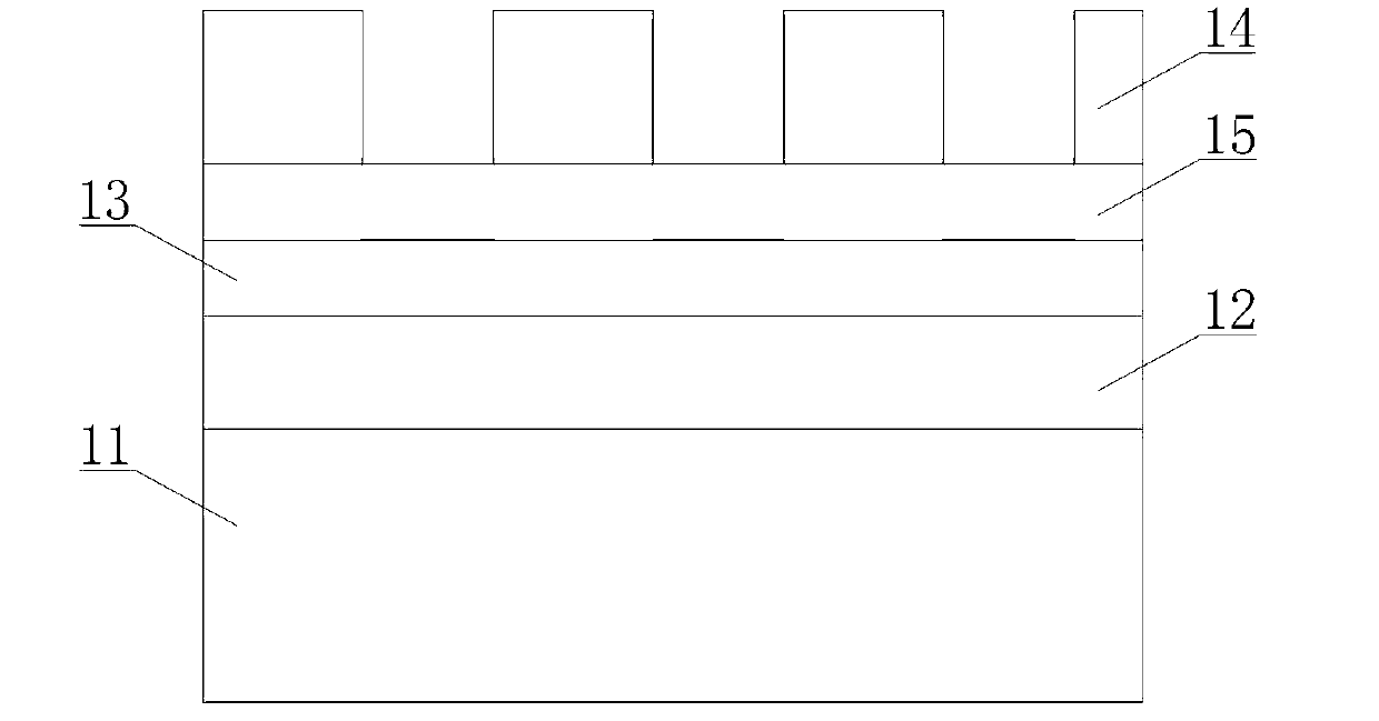
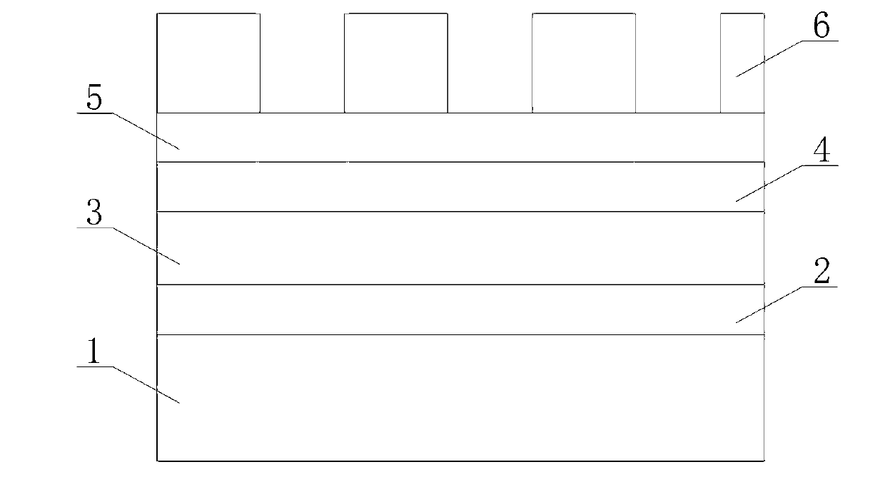
[0026] The specific embodiment of the present invention will be further described below in conjunction with accompanying drawing:

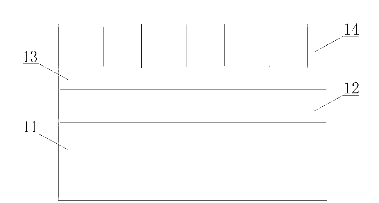
[0027] Figure 3-6 It is a schematic structural flow diagram of an embodiment in the lithography rework etching process of the present invention; as Figure 3-6 As shown, it is applied to a semiconductor stack structure that needs photolithography rework. The semiconductor stack structure is a structure that does not meet the process requirements and needs photolithography rework after the photolithography process; as shown in FIG. image 3 As shown, the semiconductor stack structure includes a silicon substrate (Si) 1, an oxide layer (Oxide) 2, a SiN layer 3, an advanced pattern film (APF) 4, a non-nitrogen bottom anti-reflection layer (N-free DARC) 5 and a Patterned photoresist (PR) 6, and silicon substrate 1, oxide layer 2 and SiN layer 3 constitute the substrate structure of the photolithographic rework etching process of the present inventio...


PUM

PropertyMeasurementUnit
Thicknessaaaaaaaaaa
Thicknessaaaaaaaaaa

Abstract

The invention relates to the technical field of integrated circuits, and in particular relates to a photoresist reworking etching process. According to the photoresist reworking etching process disclosed by the invention, in an etching process manufacturing procedure, a photoresist needing to be reworked and a non-nitrogen bottom anti-reflecting layer are sequentially removed, a new non-nitrogen bottom anti-reflecting layer is re-deposited, and the photoresist is continuously coated for performing a subsequent photoetching process so as to complete a photoresist reworking process. Therefore, during the photoetching process, preparation of a protection layer on the non-nitrogen bottom anti-reflecting layer for preventing optical parameters or surface properties of the non-nitrogen bottom anti-reflecting layer from being influenced during subsequent photoetching reworking is eliminated, so that the flow of the whole photoetching process is simplified; meanwhile, by the adoption of the photoresist reworking etching process, the accuracy of a product subjected to photoresist reworking in a subsequent photoetching process remains unchanged, and the performance and yield of the product are further improved.

Description

technical field [0001] The invention relates to the technical field of integrated circuits, in particular to a photolithography rework etching process. Background technique [0002] In the traditional integrated circuit manufacturing process, the material of the bottom anti-reflective layer (DARC Layer) used is SiON, but because SiON containing N will directly cause poisoning of the photoresist (PR) coated subsequently, the so-called The footing effect (PR footing), which in turn affects the precision of the photolithography process; in order to eliminate the above-mentioned footing effect, a layer of oxide cap layer (oxide cap layer) is generally grown on the surface of the bottom anti-reflection layer made of SiON ), to reduce the effect of N on the photoresist. [0003] At present, with the development of integrated circuit process technology, advanced patterning film (APF for short) will be involved in the lithography process at the technology node of 45nm and below; f...

Claims


Application Information

Patent Timeline
IPC IPC(8): G03F7/42H01L21/311
Inventor 雷通
Owner SHANGHAI HUALI MICROELECTRONICS CORP
Why Eureka
Try Eureka