Method and structure for three-dimensional packaging based on TSV

A three-dimensional packaging and packaging structure technology, which is applied in the manufacturing of electrical components, electrical solid-state devices, semiconductor/solid-state devices, etc. Effect

Active Publication Date: 2013-10-09
NAT CENT FOR ADVANCED PACKAGING
View PDF7 Cites 14 Cited by
  • Summary
  • Abstract
  • Description
  • Claims
  • Application Information

AI Technical Summary

Problems solved by technology

However, the biggest challenge of this method is that after the molding process, due to the mismatch of the coefficient of thermal expansion (CTE) between the molding compound and the wafer and chip, it is easy to generate large warpage
Aiming at the warping phenomenon that is easy to occur during the wafer packaging process, the document with the patent number CN102194652A discloses a method for introducing specific ions to prevent wafer warping, but a special method is required to calculate the amount of introduced ions, and the wafer must be High temperature annealing process, the process is more complicated
Japanese Patent Publication No. "JP 2003-160395" also discloses the introduction of high-concentration impurities such as germanium and oxygen into the wafer to enhance its anti-warping characteristics, which also has the disadvantages of complex process and high cost.
[0004] In the existing patent documents and other technical documents, there is no precedent for improving the technical solutions for the above problems.

Method used


Image

  • Method and structure for three-dimensional packaging based on TSV
  • Method and structure for three-dimensional packaging based on TSV
  • Method and structure for three-dimensional packaging based on TSV

Examples


Embodiment Construction

[0027] As mentioned in the background technology, for the existing wafers based on TSV packaging technology, during the packaging process, due to the difference in thermal expansion coefficient between the plastic packaging material and the wafer itself, it is easy to cause excessive stress on the wafer during the packaging process resulting in wafer warpage. Facing this problem, some existing technical solutions need to inject some dopants into the wafer to change the warping characteristics of the wafer. However, these technical solutions are not only complicated in process and high in cost, but also easily bring some additional quality problems to the wafer after modification.

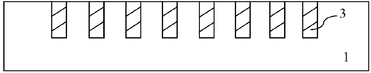
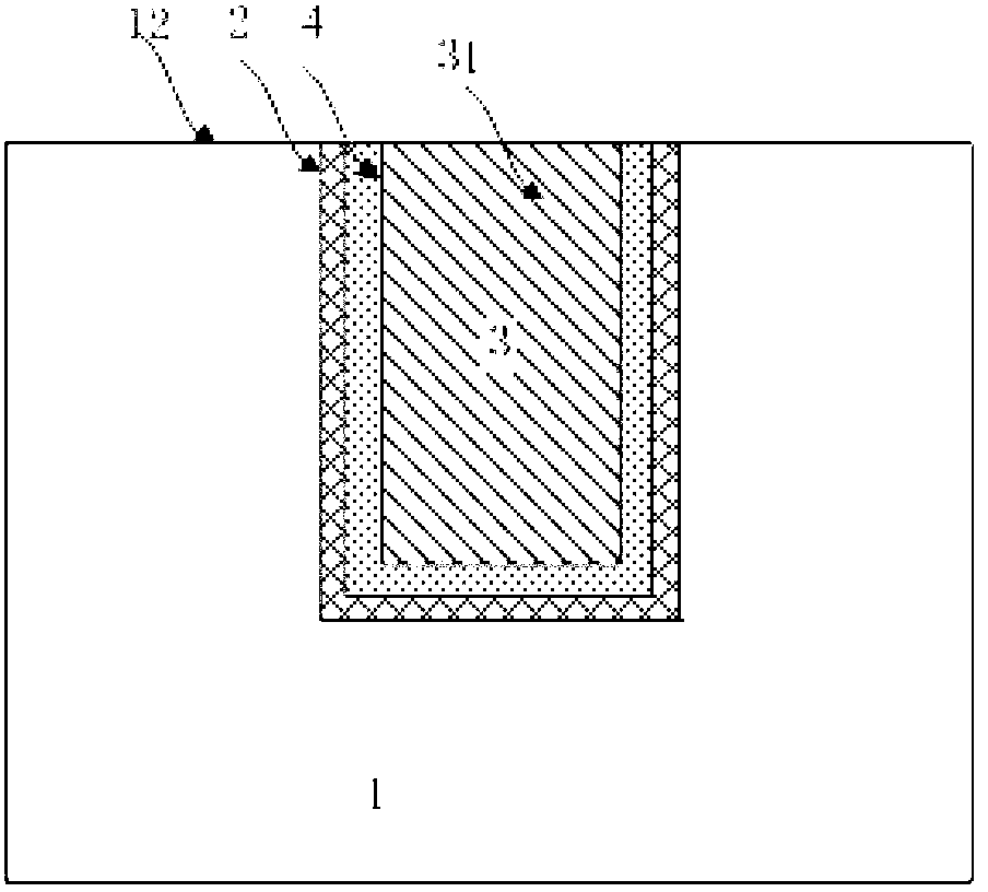
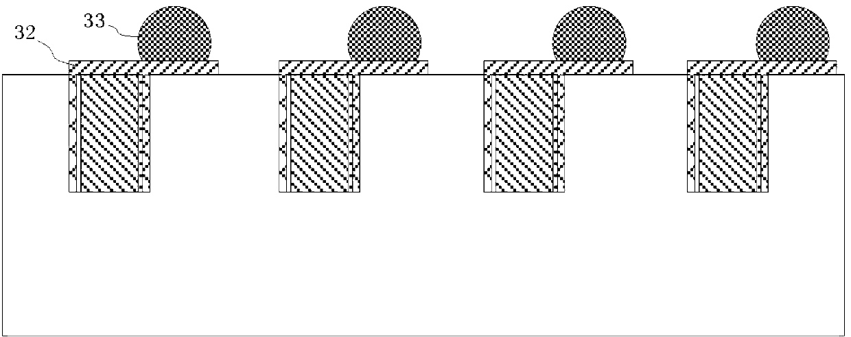
[0028] Therefore, aiming at the defects in the prior art, the present invention proposes a new low-stress three-dimensional packaging structure and method based on TSV technology. The TSV packaging structure is provided with at least two layers of different plastic encapsulants on the wafer and the ...


PUM


Abstract

The invention provides a method and structure for three-dimensional packaging based on TSV. The technology that plastic packaging is conducted on a wafer and a chip for at least twice is adopted by the method and structure for three-dimensional packaging based on the TSV. A first plastic packaging layer and a following plastic packaging layer are sequentially covered. The coefficients of thermal expansion of every two adjacent layers of plastic packaging materials are different, so that the stress generated by one of every two layers of the plastic packaging materials in the plastic packaging process is different from that generated by the adjacent layer of the plastic material in direction, the stress is counteracted between every two adjacent layers, the action force of the plastic materials to the washer is reduced, the effect that the warping degree of the washer is reduced is achieved, and therefore the smooth implementation of the non-substrate washer thinning technology is guaranteed.

Description

technical field [0001] The invention relates to a TSV wafer back thinning technical process in the field of microelectronic packaging, in particular to a multi-layer plastic packaging process to reduce the warpage problem after wafer thinning. Background technique [0002] With the continuous advancement of microelectronics technology, the feature size of integrated circuits has been continuously reduced and the interconnection density has been continuously increased. At the same time, users' requirements for high performance and low power consumption continue to increase. In this case, the way to improve the performance by further reducing the line width of the interconnection is limited by the physical characteristics of the material and the equipment process, and the resistance-capacitance (RC) delay of the two-dimensional interconnection gradually becomes the limit to improve the performance of the semiconductor chip. bottleneck. The Through Silicon Via (TSV) process c...

Claims


Application Information

Patent Timeline
Patent Type & Authority Applications(China)
IPC IPC(8): H01L21/56H01L23/31
CPCH01L24/97H01L21/568H01L2224/16H01L2224/97H01L2924/18161H01L2224/81
Inventor 张文奇何洪文王磊
Owner NAT CENT FOR ADVANCED PACKAGING
Why Eureka
Try Eureka