Backside illuminated CMOS image sensor and method for manufacturing same

A technology of image sensor and manufacturing method, which is applied in the direction of radiation control devices, etc., can solve problems such as low quantum conversion efficiency and cross-pixel interference, and achieve the effect of improving quantum conversion efficiency

Active Publication Date: 2013-10-09
OMNIVISION TECH (SHANGHAI) CO LTD
View PDF4 Cites 1 Cited by
  • Summary
  • Abstract
  • Description
  • Claims
  • Application Information

AI Technical Summary

Problems solved by technology

That is to say, the structure of the traditional front-illuminated CMOS image sensor makes the incident light need to pass through the dielectric layer (dielectric layer) and the metal layer (metal layer) before reaching the photo-sensing area, which leads to the traditional CMOS image sensor Need to face low quantum efficiency (quantum efficiency), serious cross talk between pixels (cross talk) and dark current (dark current), etc.

Method used


Image

  • Backside illuminated CMOS image sensor and method for manufacturing same
  • Backside illuminated CMOS image sensor and method for manufacturing same
  • Backside illuminated CMOS image sensor and method for manufacturing same

Examples


Embodiment Construction

[0032] The back-illuminated CMOS image sensor proposed by the present invention and its manufacturing method will be further described in detail below with reference to the accompanying drawings and specific embodiments. Advantages and features of the present invention will be apparent from the following description and claims. It should be noted that all the drawings are in a very simplified form and use imprecise scales, and are only used to facilitate and clearly assist the purpose of illustrating the embodiments of the present invention.

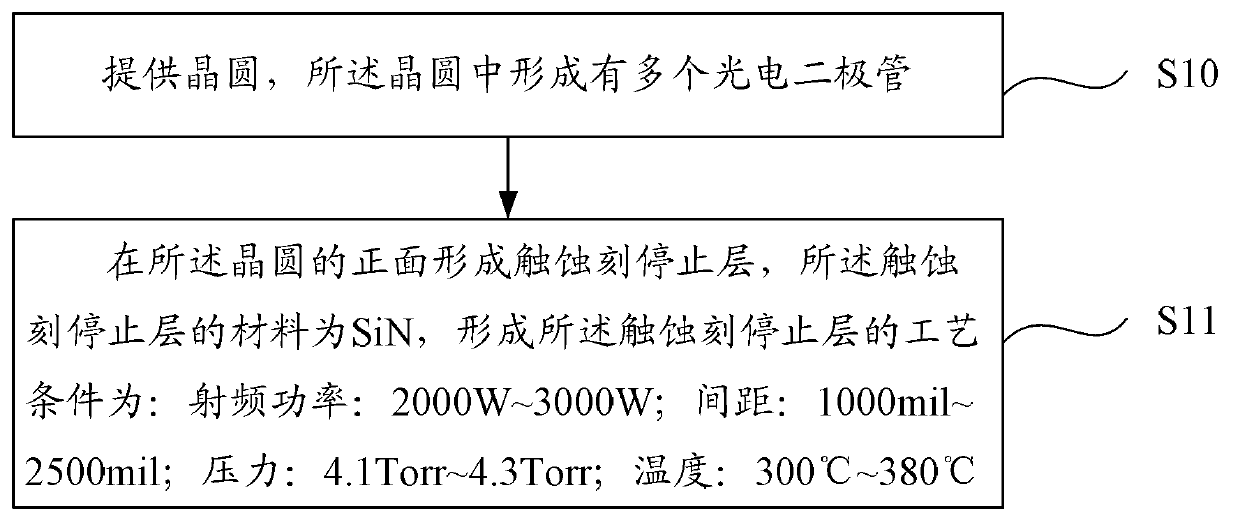
[0033] Please refer to figure 1 , which is a schematic flowchart of a manufacturing method of a back-illuminated CMOS image sensor according to an embodiment of the present invention. Such as figure 1 As shown, the manufacturing method of the back-illuminated CMOS image sensor comprises:

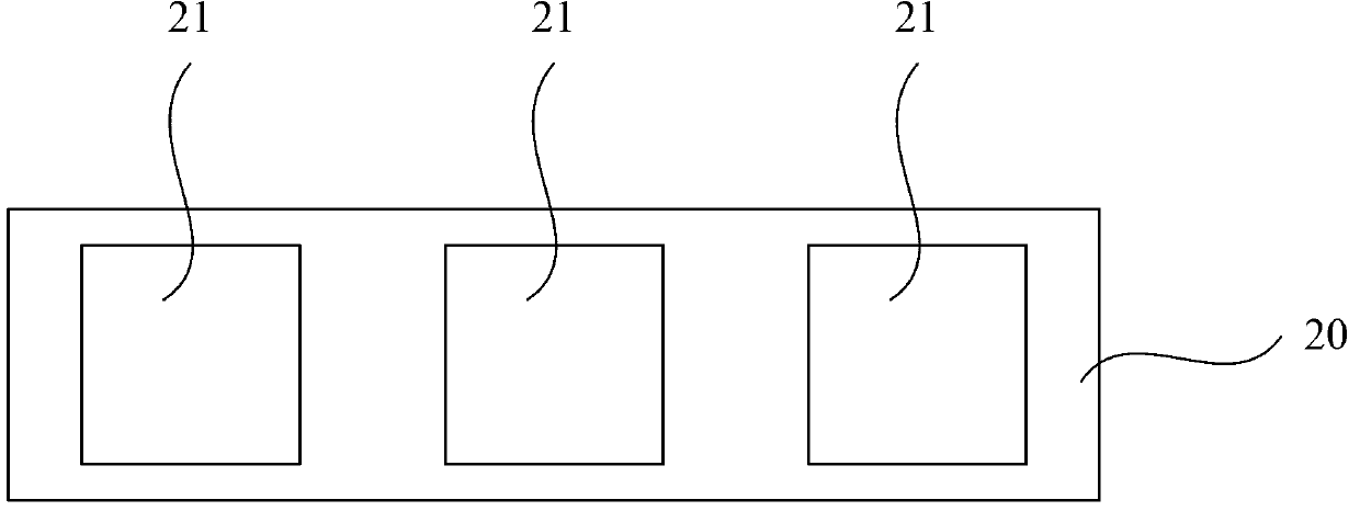
[0034] S10: providing a wafer in which a plurality of photodiodes are formed;

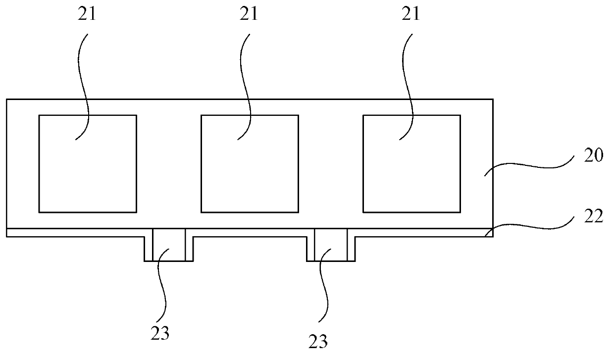
[0035] S11: forming a contact etch stop layer (contact etch stop l...


PUM


Abstract

The invention provides a backside illuminated CMOS image sensor and a method for manufacturing the backside illuminated CMOS image sensor. The method comprises the steps that a wafer is provided, and a plurality of photodiodes are formed in the wafer; a touch etching stop layer is formed in the front of the wafer; the materials of the touch etching stop layer is SiN, and technological conditions for forming of the touch etching stop layer comprise 2000W-3000W radio-frequency power, a 1000mil-2500mil gap, 4.1Torr-4.3Torr pressure and a 300 DEG C-380 DEG C temperature. Due to the mode, the touch etching stop layer in the backside illuminated CMOS image sensor has high reflectivity, light irradiating on the backside illuminated CMOS image sensor can be well reflected in the photodiodes, and quantum converting efficiency is improved.

Description

technical field [0001] The invention relates to the technical field of image sensors, in particular to a back-illuminated CMOS image sensor and a manufacturing method thereof. Background technique [0002] Image sensors can be divided into charge-coupled device (Charge-Coupled Device) image sensors (commonly known as CCD image sensors) and CMOS (Complementary Metal Oxide Semiconductor) image sensors according to the principle they use. CMOS image sensors are based on complementary metal Manufactured using oxide semiconductor (CMOS) technology. Since the CMOS image sensor is manufactured using a traditional CMOS circuit process, the image sensor and its required peripheral circuits can be integrated. [0003] Traditional CMOS image sensors use Front Side Illumination (FSI) technology to manufacture pixels on the pixel array, and the incident light needs to pass through the front side of the pixel to reach the photo-sensing area. That is to say, the structure of the traditio...

Claims


Application Information

Patent Timeline
Patent Type & Authority Applications(China)
IPC IPC(8): H01L27/146
Inventor 费孝爱叶菁
Owner OMNIVISION TECH (SHANGHAI) CO LTD
Why Eureka
Try Eureka