Four-knot cascade solar cell with Si substrate and preparation method thereof

A solar cell, four-junction technology, applied in circuits, photovoltaic power generation, electrical components, etc., can solve the problems of difficult to improve crystal quality, increase battery cost, environmental pollution, lattice mismatch, etc., to solve the problem of lattice mismatch. , The effect of reducing preparation cost and crystal quality assurance

Active Publication Date: 2013-10-09
SUZHOU INST OF NANO TECH & NANO BIONICS CHINESE ACEDEMY OF SCI
View PDF7 Cites 8 Cited by
  • Summary
  • Abstract
  • Description
  • Claims
  • Application Information

AI Technical Summary

Problems solved by technology

Due to the 2.1% lattice mismatch between 1.0eV InGaAs and GaAs, its crystal quality is difficult to improve
For example, from the perspective of lattice matching, the bonding of GaInP / GaAs (1.9eV / 1.42eV) based on GaAs substrate and InGaAsP / InGaAs (1.05eV / 0.74eV) of InP substrate is used to bond double junction cells, wafer bonded cells Two substrates, GaAs and InP, are required. Conventional wafer bonding technology requires GaAs and InP two substrates with a larger thickness (about 350 μm) to grow, which increases the cost of the battery and pollutes the environment.

Method used


Image

  • Four-knot cascade solar cell with Si substrate and preparation method thereof

Examples


Embodiment Construction

[0023] In order to make the above objects, features and advantages of the present invention more obvious and easy to understand, the following will be further described in conjunction with specific embodiments of the present invention.

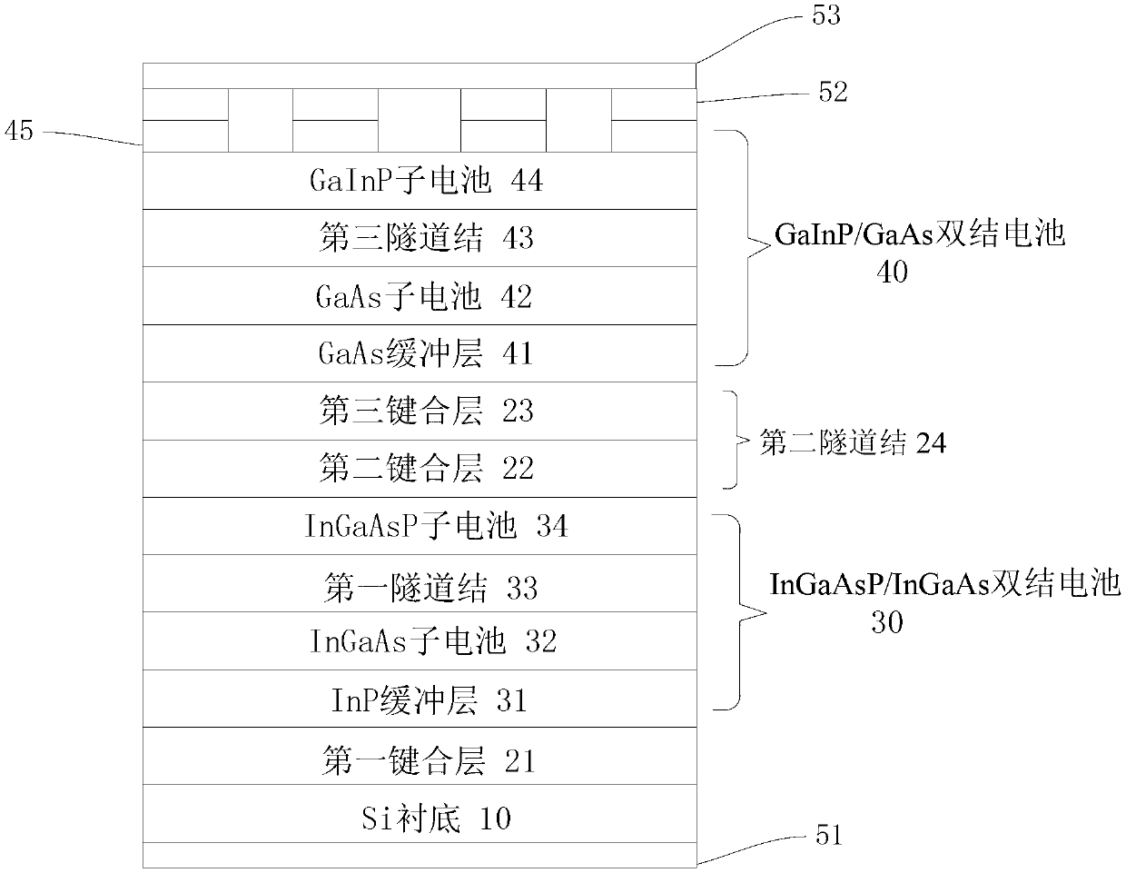
[0024] This embodiment provides a Si substrate four-junction cascaded solar cell, such as figure 1 as shown,

[0025] It includes a first bonding layer 21, an InGaAsP / InGaAs double-junction cell 30, a second bonding layer 22, a third bonding layer 23, and a GaInP / GaAs double-junction cell 40 arranged on the Si substrate 10 in sequence from bottom to top, The InGaAsP / InGaAs double-junction cells 30 and the GaInP / GaAs double-junction cells 40 are connected in series on the Si substrate 10 . It also includes a back electrode 51 and a gate electrode 52 respectively formed on the bottom of the Si substrate 10 and the top of the GaInP / GaAs double-junction cell 40 , and an anti-reflection film 53 evaporated on the surface of the gate electrode 52 . ...


PUM


Abstract

The invention relates to the field of a semiconductor technology, in particular to a four-knot cascade solar cell which comprises a first bonding layer, an InGaAsP / InGaAs double-knot cell, a second bonding layer, a third bonding layer and a GaInP / GaAs double-knot cell, wherein the first bonding layer, the InGaAsP / InGaAs double-knot cell, the second bonding layer, the third bonding layer and the GaInP / GaAs double-knot cell are arranged from bottom to top in sequence on a Si substrate. The InGaAsP / InGaAs double-knot cell and the GaInP / GaAs double-knot cell are connected in series on the Si substrate. The invention further provides a preparation method for the solar cell. The Si substrate used as the supporting substrate has good mechanical strength. Meanwhile, the method that the double-knot cells are subjected to bonding and then growing thin layers are assembled on the double-knot cells is adopted, the GaAs and InP thin layer bonding method achieves lattice match growth of the four-knot cell, and the crystalline quality of materials is guaranteed compared with lattice mismatch growth.

Description

technical field [0001] The invention relates to the technical field of semiconductor materials, in particular to a structure of a four-junction cascaded solar cell and a preparation method thereof. Background technique [0002] As an ideal green energy material, solar cells have become a research hotspot in various countries. In order to promote the further practical application of solar cells, improving their photoelectric conversion efficiency is an effective means to reduce the cost of power generation. The use of sub-cells with different bandgap widths in series in stacked cells can greatly improve the utilization rate of sunlight. At present, the system with more research and more mature technology is the GaInP / GaAs / Ge triple-junction cell. The highest conversion efficiency achieved so far is 32-33%. However, the Ge-bottom cell in the triple-junction cell covers a wider spectrum, and its short-circuit current is relatively large. In order to achieve current matching wi...

Claims


Application Information

Patent Timeline
Patent Type & Authority Applications(China)
IPC IPC(8): H01L31/0687H01L31/0693H01L31/18
CPCY02E10/544Y02P70/50
Inventor 赵勇明董建荣李奎龙孙玉润曾徐路于淑珍赵春雨杨辉
Owner SUZHOU INST OF NANO TECH & NANO BIONICS CHINESE ACEDEMY OF SCI
Why Eureka
Try Eureka