Wafer level scribing method for CIS (Cmos image sensor) product

A wafer-level, wafer-level technology, which is applied in the field of semiconductor packaging, can solve the problems of easy chipping of glass sheet cutting edges, large consumption of consumables, and affecting product quality, etc., to improve scribing efficiency, simplify the process, and improve cutting quality effect

Inactive Publication Date: 2013-10-23
JIANGYIN CHANGDIAN ADVANCED PACKAGING CO LTD
View PDF19 Cites 20 Cited by
  • Summary
  • Abstract
  • Description
  • Claims
  • Application Information

AI Technical Summary

Problems solved by technology

[0003]1. Since CIS products are small in size and relatively thick, in order to meet the cutting requirements of dicing grooves, the blades are required to be thinner, so the cutting speed is very slow, generally between 2~ 8mm/s, exceeding 10mm/s;
[0004]2. The blade cuts the glass sheet. Because the glass is brittle, the cutting edge of the glass sheet is easy to collapse, which affects the product quality;
[0005]3. Due to the large difference in the material properties of the glass sheet, silicon sheet and adhesive layer, the blade has to act on both the glass sheet and the silicon sheet, making the blade life Short, a blade gene

Method used


Image

  • Wafer level scribing method for CIS (Cmos image sensor) product
  • Wafer level scribing method for CIS (Cmos image sensor) product
  • Wafer level scribing method for CIS (Cmos image sensor) product

Examples


Embodiment 1

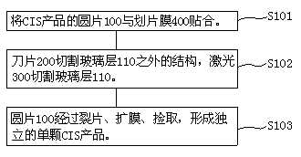
[0072] Embodiment 1, a wafer-level scribing method for a CIS product of the present invention, see Figure 3 to Figure 8 .

[0073] A wafer-level scribing method for a CIS product of the present invention comprises the following process:

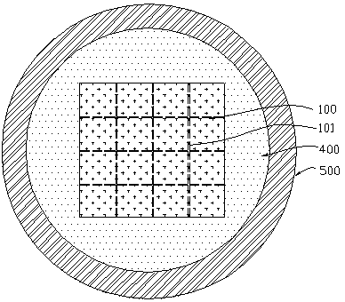
[0074] Step 1. Place the glass layer 110 of the wafer 100 of the CIS product facing down on the film lamination equipment, and the glass layer 110 is bonded to the dicing film 400 on the wafer ring 500 . The wafer ring 500 is used to fix the dicing film 400. The dicing film 400 is a UV film. The UV film has a high viscosity and can be used to stick the wafer 100. The increased viscosity will reduce, so as to facilitate the peeling off of the subsequent wafer 100; as image 3 and Figure 4 shown.

[0075] Step 2. Place the above-mentioned wafer 100 in the dicing equipment. After leveling and aligning, use the blade 200 to cut the silicon base layer 130 and the adhesive layer 120 along the dicing groove I101 of the wafer 100 according to t...

Embodiment 2

[0079] Embodiment 2, a wafer-level scribing method for a CIS product of the present invention, see Figure 9 to Figure 14 .

[0080] A wafer-level scribing method for a CIS product of the present invention comprises the following process:

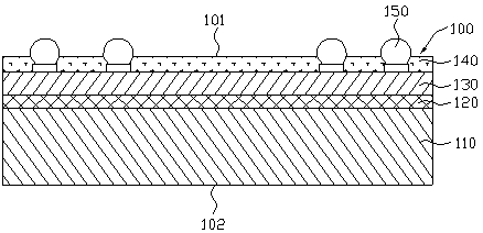
[0081] Step 1, place the glass layer 110 of the wafer 100 of the CIS product facing upwards and the solder ball layer 150 downward on the film lamination equipment, and the solder ball layer 150 is bonded to the UV scribing film 400 on the wafer ring 500; Figure 9 and Figure 10 shown.

[0082] Step 2. Place the above-mentioned wafer 100 on the laser equipment. After leveling and aligning, cut the glass layer 110 along the scribing groove II 102 of the wafer 100 with the stealth cutting technology of the laser 300 according to the travel program set by the laser 300 ;Such as Figure 11 shown.

[0083] Step 3, use UV light to peel off the dicing film 400 on the solder ball layer 150 completed in step 1 from the solder ball layer 150 of...

Embodiment 3

[0087] Embodiment three, a wafer-level scribing method for CIS products of the present invention, see Figure 15 to Figure 19 .

[0088] A wafer-level scribing method of a CIS product of the present invention comprises the following process:

[0089] Step 1. Place the CIS product wafer 100 with the solder ball layer 150 facing up and the glass layer 110 facing down on the film lamination equipment, and the glass layer 110 is bonded to the dicing film 400 on the wafer ring 500 . The dicing film 400 adopts the UV film of the model Adwill D-821HS produced by Lintec, and its film thickness is 85 microns, which can not only support the wafer 100, but also have a good penetrability to 1064nm laser light. , wherein more than 80% of the laser beam can pass through the UV film, so that the laser can perform stealth cutting on the glass under the scribing film 400 . And common dicing film 400 has more than 90% reflectivity to laser beam, has stopped laser to the cutting action of glas...


PUM

PropertyMeasurementUnit
Film thicknessaaaaaaaaaa

Abstract

The invention relates to a wafer level scribing method for a CIS (Cmos image sensor) product, and belongs to the technical field of semiconductor packaging. The wafer level scribing method for the CIS product comprises the following processes: attaching a wafer (100) of the CIS product to a scribing film (400); cutting a structure except a glass layer (110) by a blade (200), and cutting the glass layer (110) by a laser (300); and performing splitting, film expansion and picking on the wafer (100) to form an independent single CIS product. The wafer level scribing method for the CIS product, provided by the invention, is high in scribing speed, good in scribing quality and low in production cost, and can be applied to a complicated product structure.

Description

Technical field [0001] The present invention involves a round -level film -grade method of a CIS product, which belongs to the semiconductor packaging technology field. Background technique [0002] Compared with the products that are encapsulated by traditional leadership, CIS IMAGE SENSOR products are compared to the traditional leading size, cheap price, and not being vulnerable to pollution during the traditional lead key packaging products.focus on.The basic structure of the image sensor is a combined structure formed by the glass and silicon through the glue key. Among them, the thickness of the glass layer of the CIS product is about 400 microns, and the thickness of the silicon base layer is about 100 microns.The combined structure of the CIS product is large, the mechanical characteristics and physical characteristics of materials are large, and the industry generally uses traditional mechanical rotation diamond sand wheel blades to cut through.There is a problem with th...

Claims


Application Information

Patent Timeline
IPC IPC(8): B23K26/38H01L21/304
Inventor 孙超罗建忠曾志华赖志明
Owner JIANGYIN CHANGDIAN ADVANCED PACKAGING CO LTD
Why Eureka
Try Eureka