Semiconductor luminescent device or module online multifunctional test system and method

A technology for multifunctional testing and light-emitting devices, which is applied in the direction of single semiconductor device testing, semiconductor working life testing, diode testing, etc., and can solve the problems that light-emitting diode devices cannot meet the needs

Active Publication Date: 2013-10-23
INST OF SEMICONDUCTORS - CHINESE ACAD OF SCI
View PDF11 Cites 10 Cited by
  • Summary
  • Abstract
  • Description
  • Claims
  • Application Information

AI Technical Summary

Problems solved by technology

[0010] 3) At present, with the continuous promotion of applications, the packaging forms of semiconductor lighting products are diversified, inclu

Method used


Image

  • Semiconductor luminescent device or module online multifunctional test system and method
  • Semiconductor luminescent device or module online multifunctional test system and method
  • Semiconductor luminescent device or module online multifunctional test system and method

Examples


Embodiment

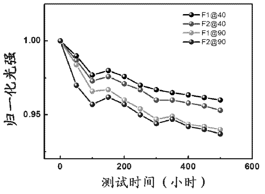
[0064] In this embodiment, the photoelectric and thermal characteristics and lifetime prediction of two different power LED devices are measured.

[0065] 1) A total of 40 different types of power LED devices (20 of each type) are placed on two different load boards, and each load board is loaded with 20 LED devices.

[0066] 2) Under the conditions of substrate temperature 25°C and current 350mA, all LED devices are tested for optical, electrical and thermal characteristics, and the data records are shown in the following table:

[0067] The test data of the first load board is shown in Table 1 below:

[0068]

[0069] Table 1

[0070] The test data of the second load board is shown in Table 2 below:

[0071]

[0072] Table 2

[0073] 2) Controlled by the central processing computer, it enters the aging mode to accelerate the aging of all LED devices. The acceleration conditions can be set to 40°C and 90°C, current 350mA, and humidity 50%. Set the aging and test int...


PUM


Abstract

The invention discloses a semiconductor luminescent device or module online multifunctional test system and method. The system comprises an electrical characteristic generation and test device, a plurality of light characteristic detection and control devices, an optical signal processing and analyzing device, a plurality of thermal characteristic detection devices, a central monitoring and processing computer, a multi-channel driving integrated control device, a plurality of acceleration multiple stress control device and a plurality of LED device-module load device. By means of the semiconductor luminescent device or module online multifunctional test system and method, the function that accelerated aging and in situ online monitoring test are conducted simultaneously in the multiple stress accelerated aging environment is achieved.

Description

technical field [0001] The invention belongs to the technical field of semiconductor light-emitting diode detection, and relates to an online multi-functional testing system and method for semiconductor light-emitting devices or modules, in particular to a controllable multi-stress condition for semiconductor light-emitting devices or modules in various packaging forms A system and method for accelerated aging and online in-situ comprehensive testing. Background technique [0002] A light emitting diode (light emitting diode, LED) is a solid light emitting device using a semiconductor chip as a light emitting material. The semiconductor material is used to form a PN junction, and in the case of an external electric field, the injected electron-hole recombination emits light, and directly converts electrical energy into light energy. Its luminous color varies with the semiconductor composition used. [0003] In 1907, Henry Joseph Round successfully prepared the first light-...

Claims


Application Information

Patent Timeline
IPC IPC(8): G01D21/02G01R31/26
CPCG01R31/2635G01R31/2642
Inventor 赵丽霞周子超杨华王军喜李晋闽
Owner INST OF SEMICONDUCTORS - CHINESE ACAD OF SCI
Why Eureka
Try Eureka