Trench VDMOS device and manufacturing method thereof

A trench type and device technology, which is applied in semiconductor/solid-state device manufacturing, semiconductor devices, electrical components, etc., can solve the problems of multiple layers of photolithography and low device cell density, so as to increase cell density and reduce manufacturing costs , the effect of reducing the number of photolithography layers

Inactive Publication Date: 2013-10-23
PEKING UNIV FOUNDER GRP CO LTD +1
View PDF6 Cites 5 Cited by
  • Summary
  • Abstract
  • Description
  • Claims
  • Application Information

AI Technical Summary

Problems solved by technology

[0010] The purpose of the present invention is to provide a trench type VDMOS device and its manufacturing method, to solve the problem that the VDMOS manufacturing process requires many layers of photolithography and the device cell density is low

Method used


Image

  • Trench VDMOS device and manufacturing method thereof
  • Trench VDMOS device and manufacturing method thereof
  • Trench VDMOS device and manufacturing method thereof

Examples


Embodiment Construction

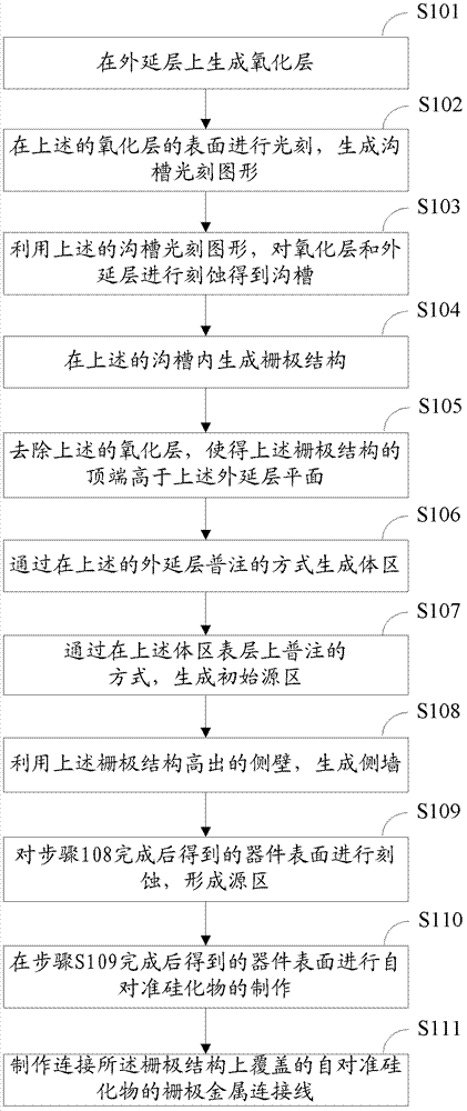
[0044] An embodiment of the present invention provides a method for manufacturing a trench-type VDMOS device, and its preferred implementation is as follows figure 1 , mainly including the following operations:

[0045] S101, forming an oxide layer 10 on the epitaxial layer.

[0046] Wherein, the above-mentioned epitaxial layer (such as N-type epitaxial layer) is made on the substrate (such as N-type substrate), and the purpose of forming the oxide layer 10 on the epitaxial layer is to make the polysilicon top of the gate structure grown in subsequent steps Higher than the plane of the epitaxial layer, the thickness of the oxide layer 10 should meet the requirement for the height of the polysilicon top of the gate structure to be higher than the plane of the epitaxial layer during subsequent processing.

[0047] S102 , performing photolithography on the surface of the above-mentioned oxide layer 10 to generate a trench photolithography pattern.

[0048] S103. Etching the oxi...


PUM


Abstract

The invention discloses a manufacturing method of a trench VDMOS device. The method comprises the steps of manufacturing a gate structure of which the top end is higher than the plane of an epitaxial layer; generating a body region and an initial source region through injection on the epitaxial layer; generating a flank by using a raised side wall of a polycrystalline silicon; etching the surface of a device to generate a source region, wherein the height of the side wall makes a part, covered by the flank, of the initial source region not etched in the etching process of the acquired source region; growing a metal layer on the surface of the device; controlling contact surfaces between the metal layer and a source electrode, between the metal layer and the body region and between the metal layer and the polycrystalline silicon to generate a silicide; and removing metal failing to react in the metal layer. The invention further provides a trench VDMOS device. As photo-etching is not required when the source region is manufactured and no contact hole needs to be manufactured, the number of photolithographic layers is reduced. Influence and restriction of factors such as photolithographic resolution and registration accuracy to the technological processes are reduced, the cellular density can be increased, and the manufacturing cost is lowered.

Description

technical field [0001] The invention relates to the technical field of the conductor chip manufacturing process, in particular to a trench type VDMOS (vertical double-diffused metal oxide semiconductor transistor) device and a manufacturing method thereof. Background technique [0002] The number of photolithographic layers in the VDMOS (Vertical Double Diffused Metal Oxide Semiconductor Transistor) device manufacturing process and the cell density of the VDMOS device have a great impact on the manufacturing cost of the VDMOS device. [0003] In the existing Trench (trench type) VDMOS device manufacturing process flow, the following four-layer structure requires photolithography: [0004] (1) When making Trench (groove), photolithography is required; [0005] (2) When making the source region, photolithography is required; [0006] (3) When making Metal (metal) and Cont (contact hole) in the source area, photolithography is required; [0007] (4) When making the metal lay...

Claims


Application Information

Patent Timeline
Patent Type & Authority Applications(China)
IPC IPC(8): H01L21/336H01L29/78H01L29/06
Inventor 马万里
Owner PEKING UNIV FOUNDER GRP CO LTD
Why Eureka
Try Eureka