A wafer-level bonding method for three-dimensional integrated packaging technology

A three-dimensional integration, wafer-level technology, applied in electrical components, semiconductor/solid-state device manufacturing, circuits, etc., can solve the reliability problems of intermetallic compounds, high temperature and pressure metal surface flatness requirements, and insufficient dense oxide layer And other issues

Active Publication Date: 2015-10-14
厦门清芯集成科技有限公司
View PDF4 Cites 0 Cited by
  • Summary
  • Abstract
  • Description
  • Claims
  • Application Information

AI Technical Summary

Problems solved by technology

Eutectic bonding is through the melting of metal alloys during the bonding process to form intermetallic compounds to complete the bonding. However, the liquid metal in this solid-liquid bonding process is difficult to meet the requirements of subsequent process conditions. At the same time, intermetallic compounds (IMC) The growth of the metal will bring reliability problems; the limitation of adhesive bonding is that the mechanical and electrical connection performance is not as good as other metal-to-metal bonding technologies; and the direct bonding process requires high process temperature and pressure as well as the flatness of the metal surface , and copper is a metal that is easily oxidized, an oxide layer will appear in a very short time when exposed to the air, and the oxide layer is not dense enough, so that oxygen can penetrate into the copper below and continue to oxidize
The oxidized surface will become uneven, which will eventually lead to an oxide layer at the bonding interface, seriously affecting the bonding strength and the performance of electrical interconnections

Method used


Image

  • A wafer-level bonding method for three-dimensional integrated packaging technology
  • A wafer-level bonding method for three-dimensional integrated packaging technology
  • A wafer-level bonding method for three-dimensional integrated packaging technology

Examples


Embodiment Construction

[0015] Specific embodiments of the present invention will be described in detail below in conjunction with the accompanying drawings. It should be understood that the specific embodiments described here are only used to illustrate and explain the present invention, and are not intended to limit the present invention.

[0016] First, if figure 1 As shown, a wafer-level bonding method for three-dimensional integrated packaging technology according to an embodiment of the present invention includes the following steps:

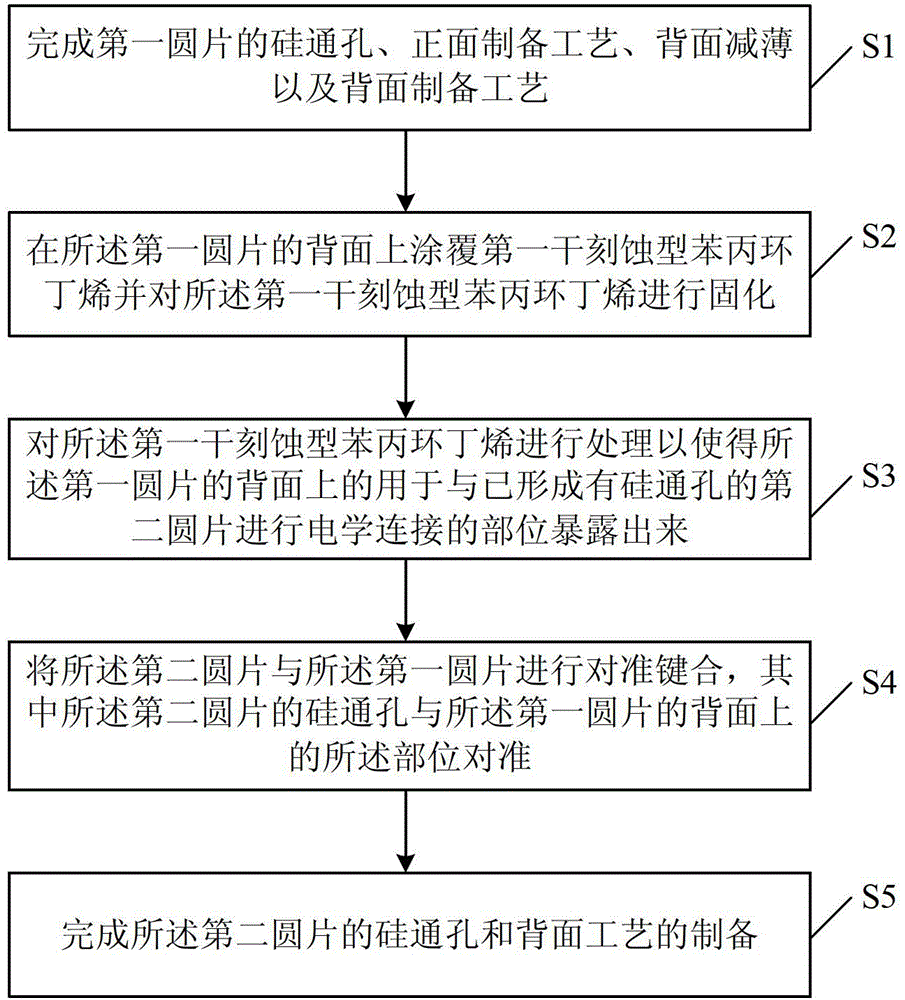
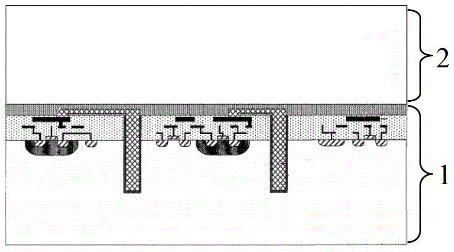
[0017] S1. Complete the through-silicon vias, front-side preparation process, back-side thinning and back-side preparation process of the first wafer;

[0018] S2. Coating a first dry-etched benzopropane (BCB) on the back surface of the first wafer and curing the first dry-etched benzopropene;

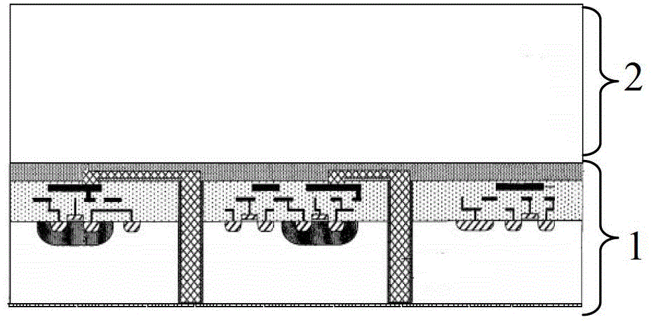
[0019] S3. Processing the first dry-etched phenylpropane to expose the portion on the back of the first wafer for electrical connection with the second wafer on which T...


PUM


Abstract

The invention aims at providing a wafer-level bonding method for a three-dimensional integrated packaging technology, belongs to a low-temperature wafer bonding method and can solve the problems that lateral deviations among bumps occur due to softening of solder at high temperatures or metal surfaces are prone to oxidization during metal bonding and the like. The method comprises the steps of finishing a process for preparing silicon through holes and front sides and a process for thinning and preparing back sides of first wafers; coating the back sides of the first wafers with first dry etching type benzocyclohutene, and curing the first dry etching type benzocyclohutene; processing the first dry etching type benzocyclohutene to expose portions on the back sides of the first wafers, which are electrically connected with second wafers in which silicon through holes are already formed; performing aligned bonding on the second wafers and the first wafers, wherein the silicon through holes of the second wafers are aligned to the portions on the back sides of the first wafers; finishing a process for preparing the silicon through holes and back sides of the second wafers.

Description

technical field [0001] The invention relates to the field of semiconductor packaging, in particular to a wafer-level bonding method for three-dimensional integrated packaging technology. Background technique [0002] With the development of semiconductor three-dimensional packaging technology, wafer-wafer bonding technology has become a current research hotspot. At present, in order to realize wafer-level conductive interconnect stacking with through-silicon vias (TSVs), the commonly used method is to realize mechanical and electrical connections between wafers through metal-metal bonding. The bonding methods between metals mainly include eutectic bonding, adhesive bonding and direct bonding. Eutectic bonding is through the melting of metal alloys during the bonding process to form intermetallic compounds to complete the bonding. However, the liquid metal in this solid-liquid bonding process is difficult to meet the requirements of subsequent process conditions. At the same...

Claims


Application Information

Patent Timeline
Patent Type & Authority Patents(China)
IPC IPC(8): H01L21/60H01L21/50
Inventor 蔡坚魏体伟王谦
Owner 厦门清芯集成科技有限公司
Why Eureka
Try Eureka