Light source adopting LED chip packaging technology

An LED chip and technology technology, applied in the field of LED optics, can solve the problems of the heat of the LED chip cannot be released in time, it is not easy to illuminate the reflector cup, and the cost of optical components is increased, so as to facilitate development and application, increase the number of chips, and increase the area. Effect

Inactive Publication Date: 2013-11-13
江西量一光电科技有限公司
View PDF9 Cites 3 Cited by
  • Summary
  • Abstract
  • Description
  • Claims
  • Application Information

AI Technical Summary

Problems solved by technology

Disclosed is an LED lamp and lamp optically treated with a reflective cup combined with a lens, which combines the reflective cup and the lens by setting an optical processing part to mix the light emitted by the LED lamp, so that the LED lamp has a spot effect, which increases the Optical device cost, lens design cost, complex structure and principle, and it is difficult to achieve good lighting effect
It combines the reflective cup and the lens by setting the optical processing part, and mixes the light emitted by the LED lamp, so that the LED lamp has a spot effect, which increases the cost of the optical device, and the structure principle is complicated, and it is difficult to achieve a good lighting effect
[0004] The existing LED-COB packaging technology only has one layer of glue, and its main defects are: 1. Because it is a planar package, the light-emitting surface is too large, it is not easy to cooperate with the reflector cup to achieve key lighting, and the reason for the large light-emitting surface causes a certain degree of damage. glare
2. There is no protective adhesive layer after solid crystal and wire bonding, and it is easy to die in the production process.
3. The packaging form of single rubber surface makes the LED chip directly contact with the phosphor powder, and the heat emitted by the LED chip cannot be released in time, which accelerates the aging of the phosphor powder and causes serious light attenuation
4. The light-emitting surface of the traditional COB packaging technology LED chip is the light-emitting surface facing away. Since the light-emitting surface of the LED chip faces outward, it may cause glare interference to people.
5. The transparent filling glue layer is covered on the LED chip protective layer, and the fluorescent glue layer is covered on the top layer. The chips emitted by the LED chip during operation cannot be well converged, and the light efficiency is low.

Method used


Image

  • Light source adopting LED chip packaging technology
  • Light source adopting LED chip packaging technology
  • Light source adopting LED chip packaging technology

Examples


Embodiment 1

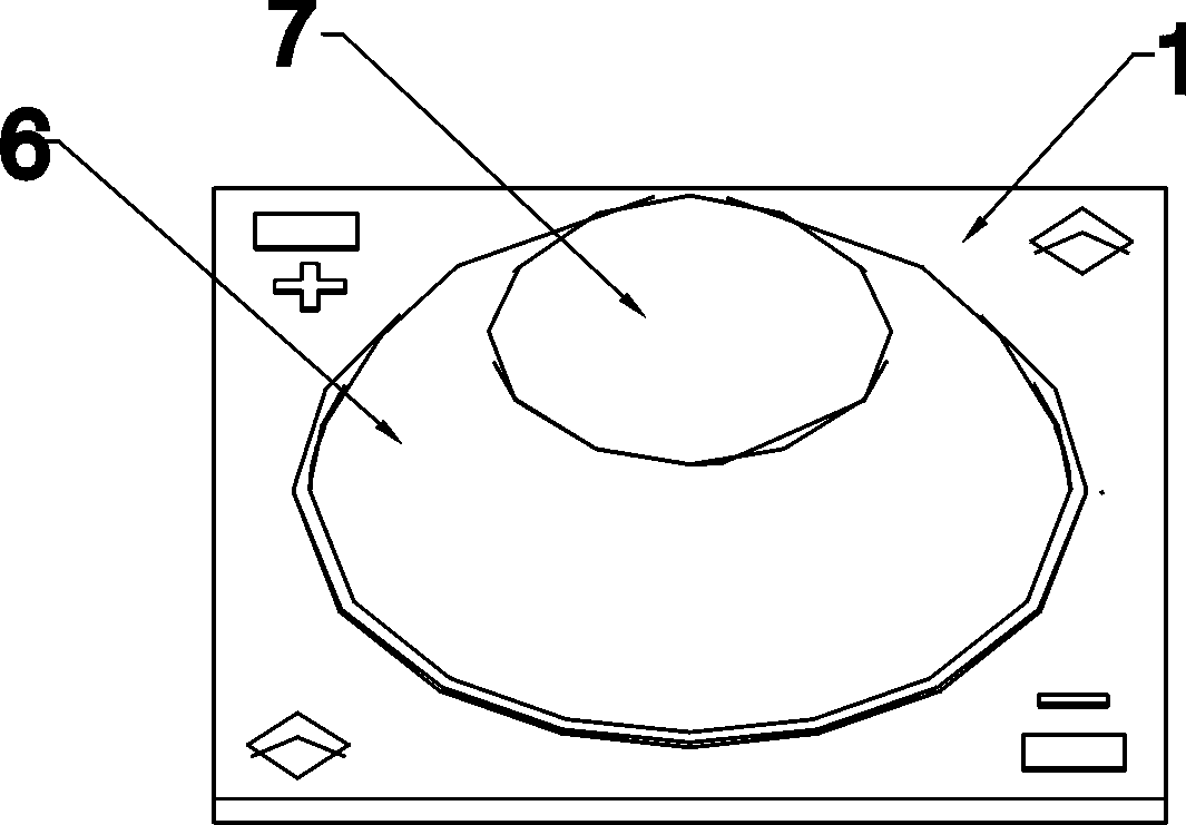
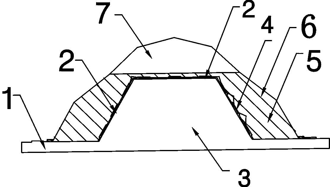
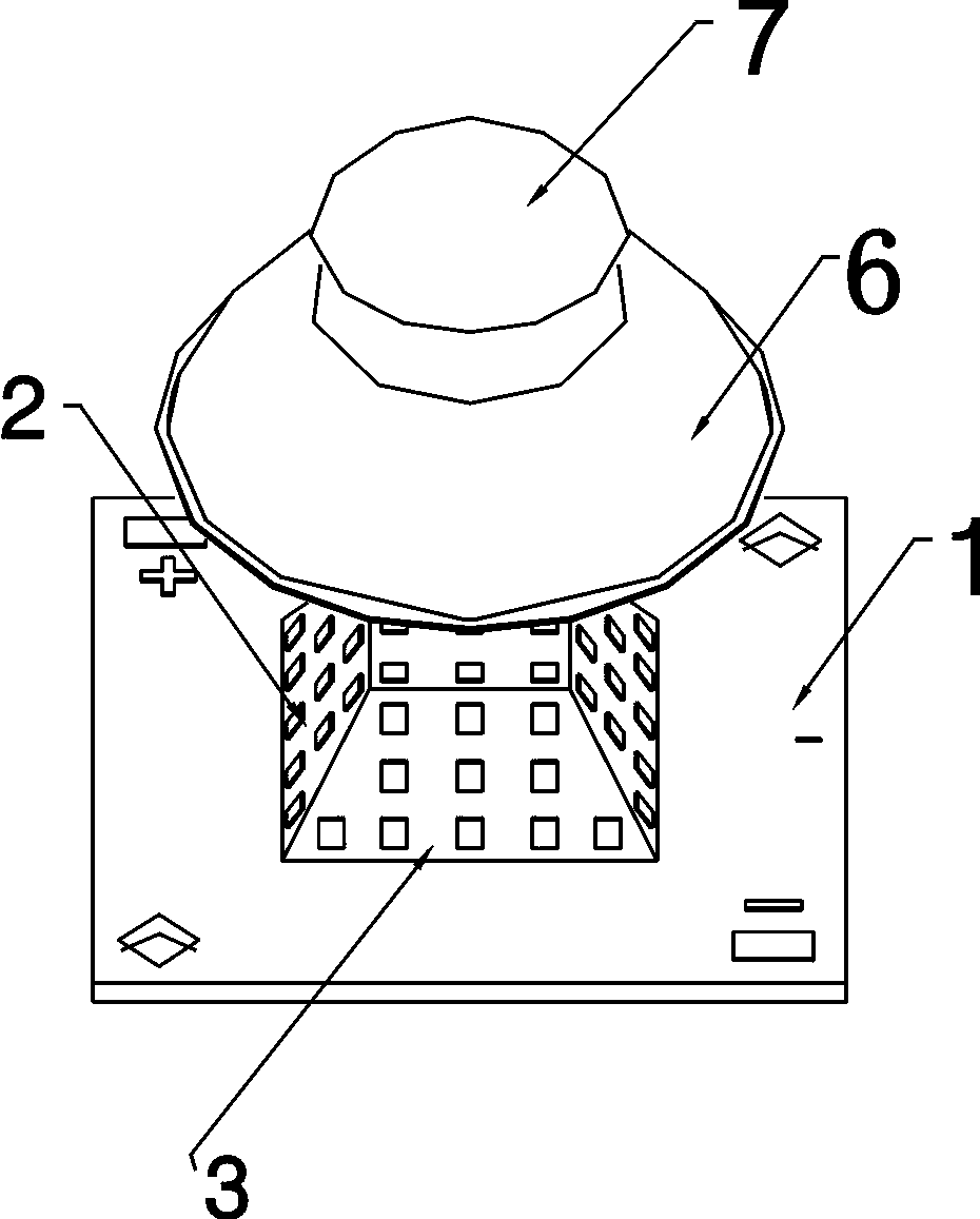
[0035] Embodiment 1: as Figure 1-4 As shown, a light source with LED chip packaging technology includes a copper substrate 1 and an LED chip 2. There is a raised portion 3 in the center of the copper substrate 1, and several LED chips 2 are fixed on the surface of the raised portion 3. The LED chip 2 is sequentially covered with a protective adhesive layer 4, a transparent filling adhesive layer 5, and a fluorescent powder adhesive layer 6 covering the entire raised portion 3, and an optical lens 7 is fixedly connected to the raised portion 3 covered by the above-mentioned adhesive layer. on top.

[0036] Specifically: the convex height part 3 is covered with LED chips 2, and each LED chip is connected with a gold wire. There are three layers of silica gel layers on the LED chip 2. From the inside to the outside, the protective adhesive layer 4, the transparent filling adhesive layer 5, and the fluorescent Powder layer 6. Phosphor glue layer is a silicone layer containing p...

Embodiment 2

[0041] Example 2: see Figure 7 , the difference from Embodiment 1 is that the optical lens 7 is a concave free-form surface.

Embodiment 3

[0042] Embodiment 3: see Figure 8 , The difference from Embodiment 1 is that the optical lens 7 is an outer irregular convex bead point.


PUM


Abstract

The invention discloses a light source adopting an LED chip packaging technology. The light source comprises a copper substrate and LED chips, wherein a bulged part is formed in the center of the copper substrate; a plurality of LED chips are fixedly connected on the surface of the bulged part; a protective adhesive layer, a transparent filling adhesive layer and a fluorescent powder adhesive layer are sequentially arranged on each LED chip; the whole bulged part is covered with the three adhesive layers; and an optical lens is fixedly connected onto the top of the bulged part covered with the adhesive layers. According to the light source adopting the LED chip packaging technology, main center light rays are converged, so that the luminous efficiency is improved; and surrounding light rays are all reflected to provide illumination, and light spots are uniform.

Description

technical field [0001] The invention relates to the technical field of LED optics, in particular to a light source of LED chip packaging technology. Background technique [0002] The existing LED-COB packaging technology, which includes the substrate, the LED chip fixed on the substrate, the apron formed on the substrate and the fluorescent powder adhesive layer in the apron, is implemented. More specifically, the existing COB surface light source The traditional form of packaging is a single-layer phosphor adhesive surface, that is, a layer of fluorescent adhesive is covered on the LED chip. [0003] In terms of application, another example is Chinese Patent No. 2010206457499, which is named: an LED lamp and lamp for optical processing with a reflective cup combined with a lens. Disclosed is an LED lamp and lamp optically treated with a reflective cup combined with a lens, which combines the reflective cup and the lens by setting an optical processing part to mix the light...

Claims


Application Information

Patent Timeline
Patent Type & Authority Applications(China)
IPC IPC(8): H01L33/48H01L33/58H01L33/64H01L25/075
Inventor 廖昆
Owner 江西量一光电科技有限公司
Why Eureka
Try Eureka