Printed circuit board and manufacturing method thereof

A technology for printed circuit boards and manufacturing methods, which is applied in the direction of printed circuit manufacturing, printed circuits, printed circuit components, etc., can solve the problems of high production cost, waste of raw materials, and filling rate less than 60%, so as to avoid production costs and Waste of raw materials, prevention of resin separation or breakage, and improvement of filling accuracy

Active Publication Date: 2013-11-13
SHANGHAI MEADVILLE ELECTRONICS
View PDF3 Cites 8 Cited by
  • Summary
  • Abstract
  • Description
  • Claims
  • Application Information

AI Technical Summary

Problems solved by technology

The traditional plugging machine and one-time filling plugging method can only ensure high-quality plugging of printed circuit boards with a thickness-to-diameter ratio of less than 6:1. For printed circuit boards with a higher thickness-to-diameter ratio, traditional processes cannot meet the requirements. The rate is very low, the fill rate of via / buried holes is less than 60%
If the filling rate of through holes or buried holes is too low, it will cause some quality problems such as line depression, tin beads in holes, green oil on the plate, etc.
Plugging holes for printed circuit boards with a thickness-to-diameter ratio greater than 6:1 requires high equipment requirements, high equipment costs, high production costs, and a lot of waste of raw materials in the production process.

Method used


Image

  • Printed circuit board and manufacturing method thereof
  • Printed circuit board and manufacturing method thereof
  • Printed circuit board and manufacturing method thereof

Examples


Embodiment 1

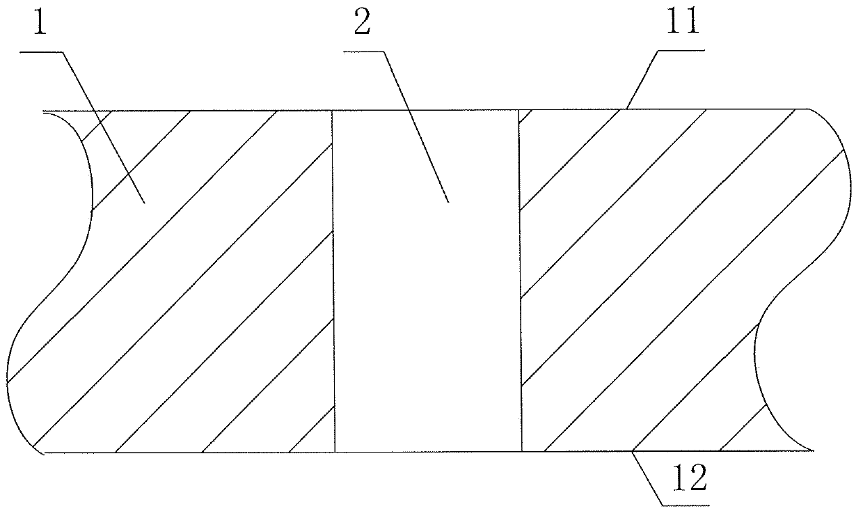
[0040] like figure 1 A cross-sectional view of the printed wiring board 1 is shown. The printed circuit board 1 is provided with through holes 2 . The through hole 2 extends from the upper surface 11 to the lower surface 12 of the printed circuit board. The ratio of the thickness of the printed circuit board 1 to the diameter of the through hole 2 is 10:1. Before filling, first bake the printed circuit board 1 at 100°C for 4 hours to remove moisture in the through hole 2 and make it dry.

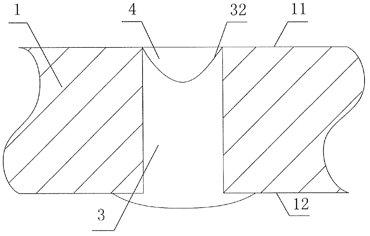
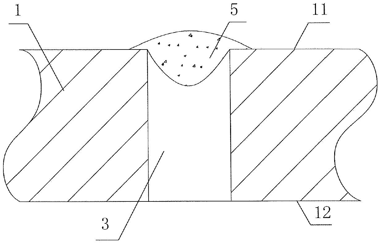
[0041]Fill the via hole 2 with a silk-screen device. Firstly, the first epoxy resin 3 with a viscosity of 20 Pa·s / 25° C. is filled into the through hole 2 . The thickness of the printing squeegee is 2cm, the hardness is 70°, and the squeegee angle is 8°. like figure 2 As shown, the first epoxy resin 3 protrudes from the lower surface 22 of the printed wiring board 1 . However, when filling with common screen printing equipment, a groove 4 is formed between the upper surface 32 of the...

Embodiment 2

[0048] like figure 1 A cross-sectional view of the printed wiring board 1 is shown. The printed circuit board 1 is provided with through holes 2 . The through hole 2 extends from the upper surface 11 to the lower surface 12 of the printed circuit board. The ratio of the thickness of the printed circuit board 1 to the diameter of the through hole 2 is 10:1. Before filling, first bake the printed circuit board 1 at 120° C. for 2.5 hours to remove moisture in the through hole 2 and make it dry.

[0049] Fill the via hole 2 with a silk-screen device. Firstly, 6458 bisphenol F type epoxy resin 3 with a viscosity of 35 Pa·s / 25° C. is filled into the through hole 2 . The thickness of the printing squeegee is 2cm, the hardness is 70°, and the squeegee angle is 8°. like figure 2 As shown, the 6458 bisphenol F type epoxy resin 3 protrudes from the lower surface 22 of the printed wiring board 1 . However, when filled with common silk screen equipment, a groove 4 is formed between...

Embodiment 3

[0056] like figure 1 A cross-sectional view of the printed wiring board 1 is shown. The printed circuit board 1 is provided with through holes 2 . The through hole 2 extends from the upper surface 11 to the lower surface 12 of the printed circuit board. The ratio of the thickness of the printed circuit board 1 to the diameter of the through hole 2 is 10:1. Before filling, first bake the printed circuit board 1 at 110° C. for 4 hours to remove moisture in the through hole 2 and make it dry.

[0057] Fill the via hole 2 with a silk-screen device. Firstly, the first epoxy resin 3 with a viscosity of 48 Pa·s / 25° C. is filled into the through hole 2 . The thickness of the printing squeegee is 2cm, the hardness is 70°, and the squeegee angle is 8°. like figure 2 As shown, the first epoxy resin 3 protrudes from the lower surface 22 of the printed wiring board 1 . However, when filling with common screen printing equipment, a groove 4 is formed between the upper surface 32 of ...


PUM


Abstract

The invention discloses a printed circuit board which is characterized by comprising at least one hole, wherein the hole is provided with at least one opening, and the hole is filled with at least one filler. The invention further discloses a manufacturing method of the printed circuit board, which is characterized by comprising the steps that the hole is filled with the first filler, and then filled with the second filler, so that the second filler and the first filler are coagulated into a whole to fully fill the hole. According to the printed circuit board, the hole is filled with at least one filler, so that a filling rate in the hole is as high as 95-100%, the product quality of the printed circuit board is improved, the manufacturing method of the printed circuit board can be compatible with the traditional equipment, and the production cost is lowered.

Description

technical field [0001] The invention relates to a printed circuit board and a manufacturing method thereof. Background technique [0002] In recent years, with the progress and development of high-density interconnected printed circuit boards and high-density laminated printed circuit boards, the application of high-density interconnected printed circuit boards has expanded from the field of single, light, thin and small mobile communications and portable devices to large-scale Emerging fields such as high-thickness communication equipment. These new fields put forward many new requirements for the manufacturing process of high-density interconnection printed circuit boards, such as interlayer alignment accuracy, hole copper thickness, hole type, plug hole quality, etc. Among them, with the increase of plate thickness and hole density, and the decrease of hole diameter, higher requirements are put forward for the ability of through / buried hole plugging. The traditional plu...

Claims


Application Information

Patent Timeline
Patent Type & Authority Applications(China)
IPC IPC(8): H05K1/02H05K3/00
Inventor 黄伟樊泽杰陶伟良
Owner SHANGHAI MEADVILLE ELECTRONICS
Why Eureka
Try Eureka