

Touch input sheet and production method thereof
A touch input and production method technology, applied in the input/output process of data processing, instruments, electrical digital data processing, etc. It can achieve the effect of realizing mass production operation, improving adhesion and improving yield
- Summary
- Abstract
- Description
- Claims
- Application Information
AI Technical Summary
Problems solved by technology
Method used
Image

Examples
Embodiment 1
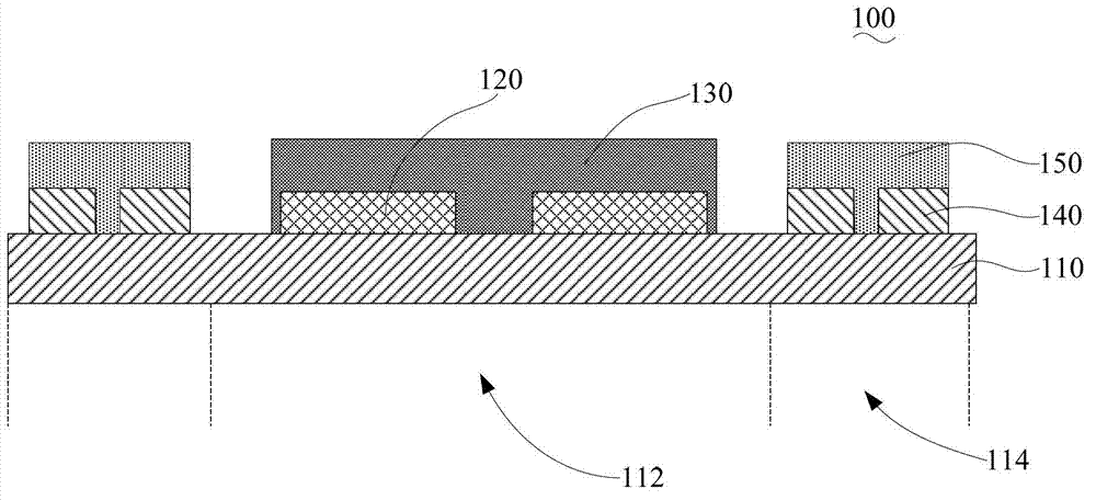
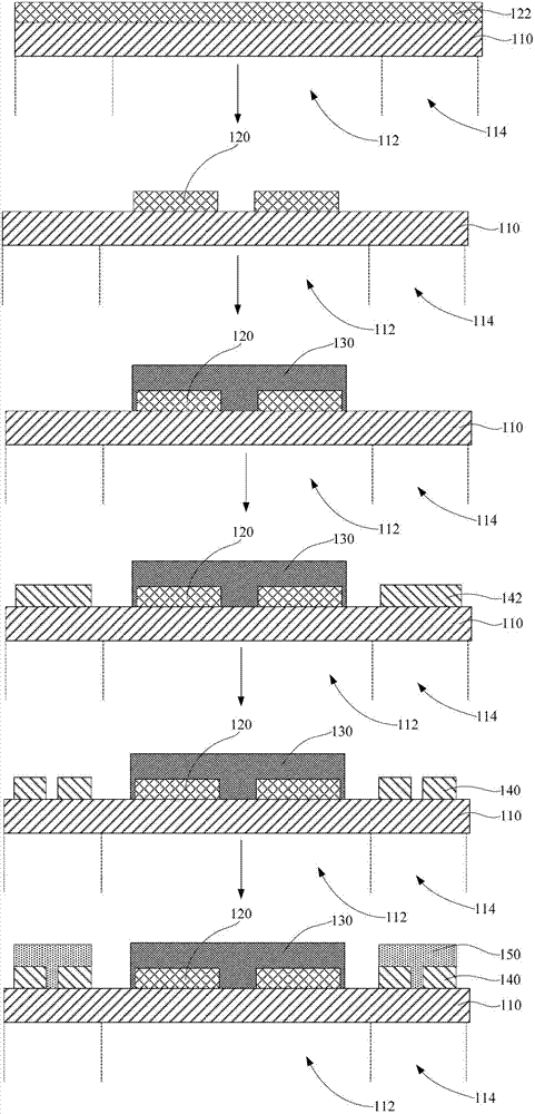
[0054] The transparent substrate uses a colorless and transparent ethylene terephthalate (PET) plastic film with a thickness of 50-125 μm, and forms ITO with a thickness of 10-30 nm as a conductive layer on its surface by sputtering. Aging treatment is carried out on the transparent substrate including the conductive layer by a high temperature of 140° C. to ensure that the stretch rate of the transparent substrate is within a normal range. Then, the conductive layer is processed by fully automatic printing to form the required conductive pattern in the visible area of the transparent substrate. The specific process is: use screen printing to print the preset conductive pattern area on the conductive layer The acid-resistant polyester is cured by ultraviolet light, and the polyester is cured by ultraviolet light; the conductive layer is etched with HCl solution, and the conductive layer in the visible area with the area other than the preset conductive pattern is etched away,...
Embodiment 2
[0057] The transparent substrate uses a colorless and transparent polybutylene terephthalate (PBT) plastic film with a thickness of 50-125 μm, and forms ITO with a thickness of 10-30 nm as a conductive layer on its surface by sputtering. Aging treatment is carried out on the transparent substrate including the conductive layer by a high temperature of 140° C. to ensure that the stretch rate of the transparent substrate is within a normal range. Then, the required circuit pattern is formed in the visible area through the yellow light process. The specific process is: coating the negative photoresist on the entire surface of the conductive layer, and exposing the negative photoresist to the preset conductive pattern area by exposure. for curing; then use K 2 CO 3 Develop the negative photoresist with an organic solution to remove the uncured negative photoresist; use HNO 3 The solution etches the conductive layer, and etch away the conductive layer with areas other than the pr...
PUM
 Abstract
Description
Claims
Application Information