Wafer-level packaging structure and packaging method of image sensor

A wafer-level packaging and image sensor technology, which is applied in the manufacture of electrical solid-state devices, semiconductor devices, semiconductor/solid-state devices, etc., can solve problems affecting the overall performance of the chip, poor light reception and emission, and light transmission.

Active Publication Date: 2013-11-20
CHINA WAFER LEVEL CSP
View PDF4 Cites 13 Cited by
  • Summary
  • Abstract
  • Description
  • Claims
  • Application Information

AI Technical Summary

Problems solved by technology

However, even if the package cover is transparent, it will still affect the transmission of light, making the reception and emission of light in the photosensitive area of ​​the image sensor difficult, thereby affecting the overall performance of the chip. Lid and Wafer Peeled Off

Method used


Image

  • Wafer-level packaging structure and packaging method of image sensor
  • Wafer-level packaging structure and packaging method of image sensor
  • Wafer-level packaging structure and packaging method of image sensor

Examples


Embodiment Construction

[0029] When using the existing wafer-level packaging technology to package the image sensor, at the end of the packaging process, the package cover needs to be peeled off from the wafer, but how can the package cover be easily and conveniently removed without damaging the wafer? There is still no effective solution to peeling off from the wafer.

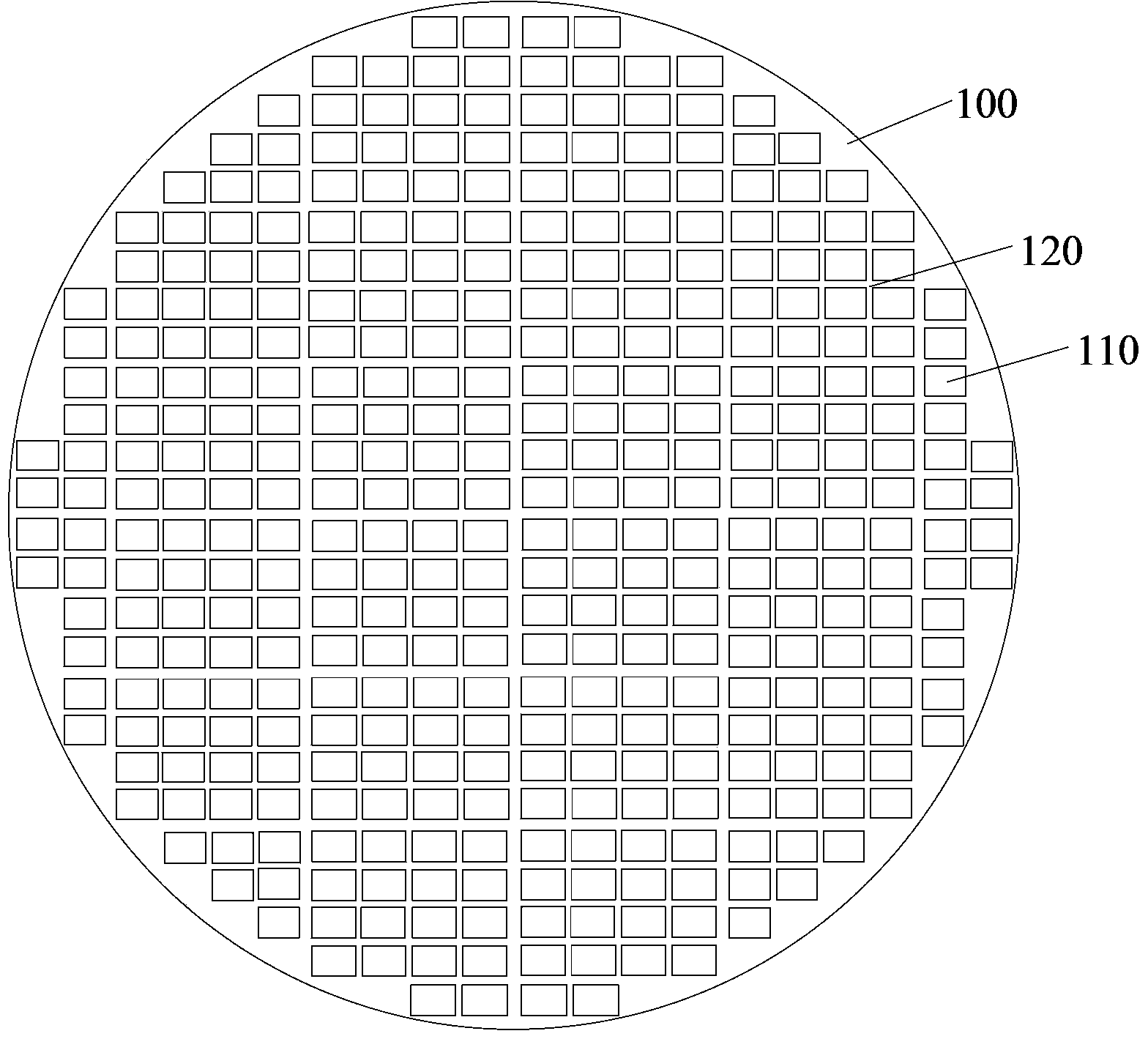
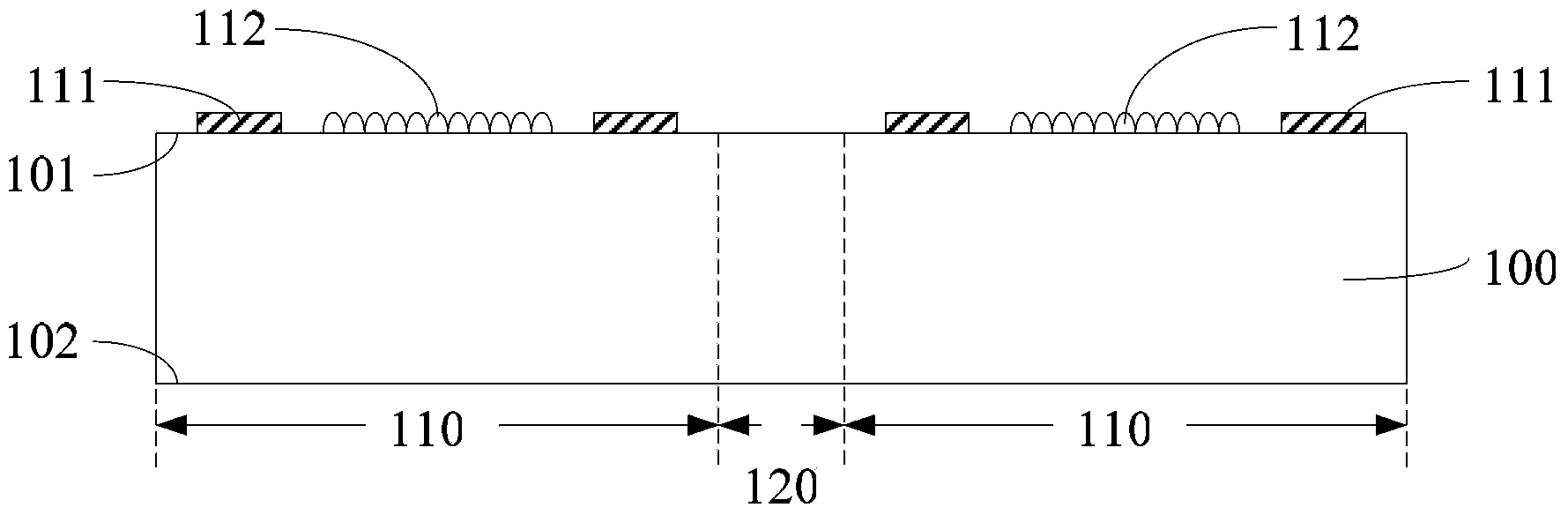
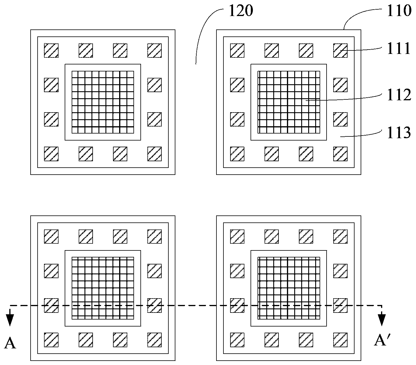
[0030] To this end, the present invention provides a wafer-level packaging structure and packaging method of an image sensor. The wafer-level packaging structure of the image sensor includes: a wafer to be packaged; a wafer located on the first surface of the wafer to be packaged and located in the chip area The pad and image sensing area inside; the first dike structure located on the surface of the pad; the package cover arranged opposite to the first surface of the wafer to be packaged, and the second dike located on the surface of the package cover structure, the position of the second dike structure corresponds to the position o...


PUM


Abstract

The invention relates to a wafer-level packaging structure and packaging method of an image sensor. The wafer-level packaging structure of the image sensor comprises a wafer to be packaged, a pad and an image sensing area which are positioned on the first surface of the wafer to be packaged and positioned in a chip region, a first cofferdam structure positioned on the surface of the pad, a packaging cover which is arranged by being opposite to the first surface of the wafer to be packaged, and a second cofferdam structure positioned on the surface of the packaging cover, wherein the position of the second cofferdam structure corresponds to that of a cutting channel region, the packaging cover and the wafer to be packaged are fixedly jointed by utilizing the second cofferdam structure, and the top surface of the first cofferdam structure is in contact with the surface of the packaging cover. According to the wafer-level packaging structure and packaging method, during the packaging process, the mechanical strength and cavity ratio between the wafer to be packaged and the packaging cover are ensured, the packaging cover can be automatically separated from the wafer to be packaged at the end of a packaging process, and the wafer to be packaged can not be damaged.

Description

technical field [0001] The invention relates to semiconductor packaging technology, in particular to a wafer-level packaging structure and packaging method of an image sensor. Background technique [0002] As the size of the image sensor becomes smaller and smaller, the number of pads increases and the spacing between the pads becomes narrower. Correspondingly, higher requirements are placed on the packaging of the image sensor. [0003] The traditional image sensor packaging method is usually packaged by wire bonding (Wire Bonding). However, with the rapid development of integrated circuits, longer leads make the product size unable to meet the ideal requirements. Therefore, Wafer Level Packaging (Wafer Level Packaging) Package, WLP) has gradually replaced wire bonding packaging as a more commonly used packaging method. Wafer Level Packaging (WLP) technology is a technology that performs packaging and testing on the entire wafer and then cuts it to obtain a single finished...

Claims


Application Information

Patent Timeline
Patent Type & Authority Applications(China)
IPC IPC(8): H01L23/18H01L21/48H01L21/50
CPCH01L27/14687H01L27/14618H01L2224/13
Inventor 王之奇喻琼王蔚
Owner CHINA WAFER LEVEL CSP
Why Eureka
Try Eureka