System and method for production of nanostructures over large areas

A plane, substrate technology, applied in the field of photolithography for the fabrication of micro or nanostructures, based on the Taber effect or self-imaging

Active Publication Date: 2013-11-20
EULITHA
View PDF7 Cites 8 Cited by
  • Summary
  • Abstract
  • Description
  • Claims
  • Application Information

AI Technical Summary

Problems solved by technology

A solution to this problem would be to use a smaller area pattern in the mask and employ a step-and-repeat exposure strategy to print on a much larger area on the substrate, but this would require a complex mechanical system in order to perform the exposure and would The subfields are a

Method used


Image

  • System and method for production of nanostructures over large areas
  • System and method for production of nanostructures over large areas
  • System and method for production of nanostructures over large areas

Examples


Embodiment Construction

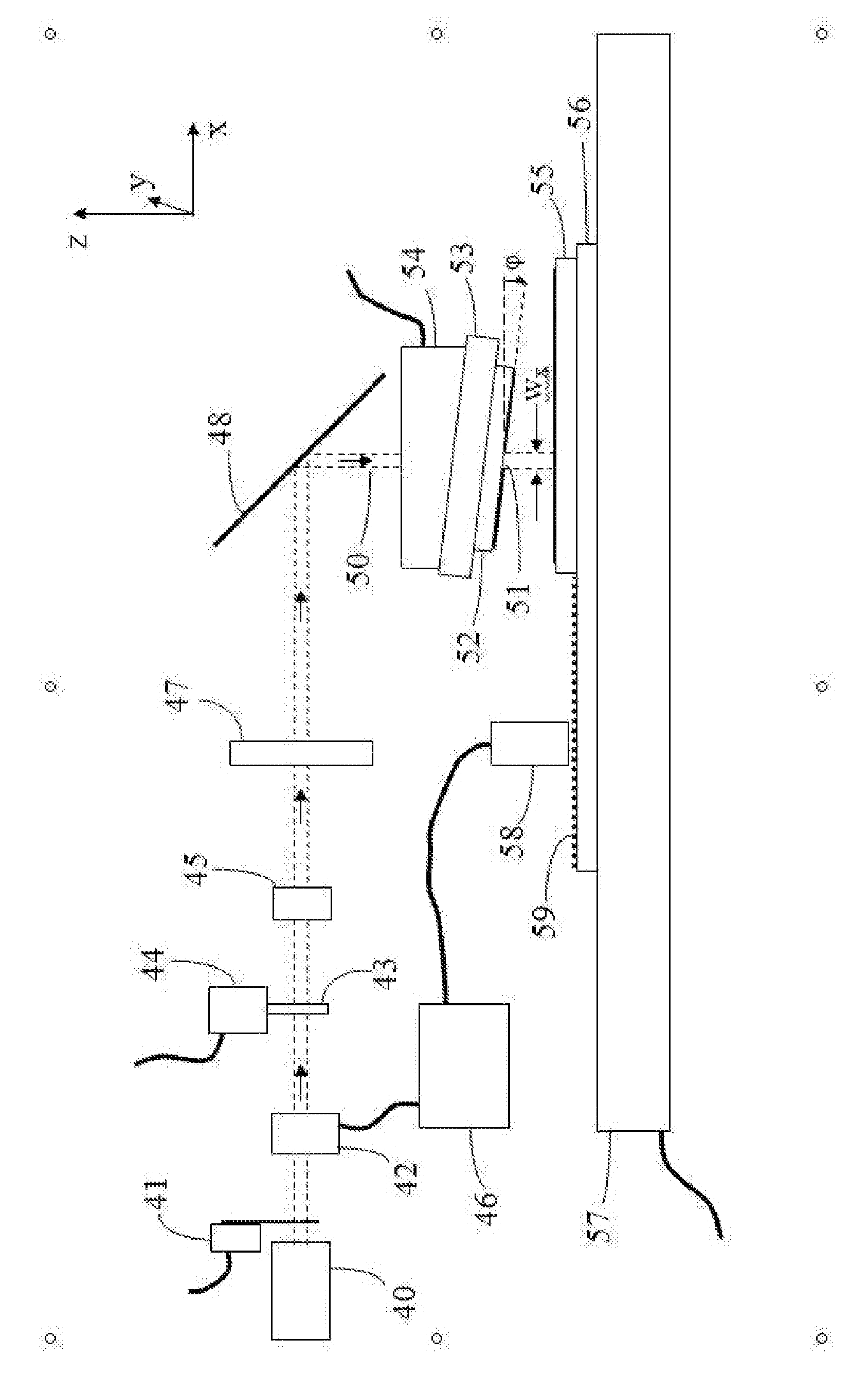
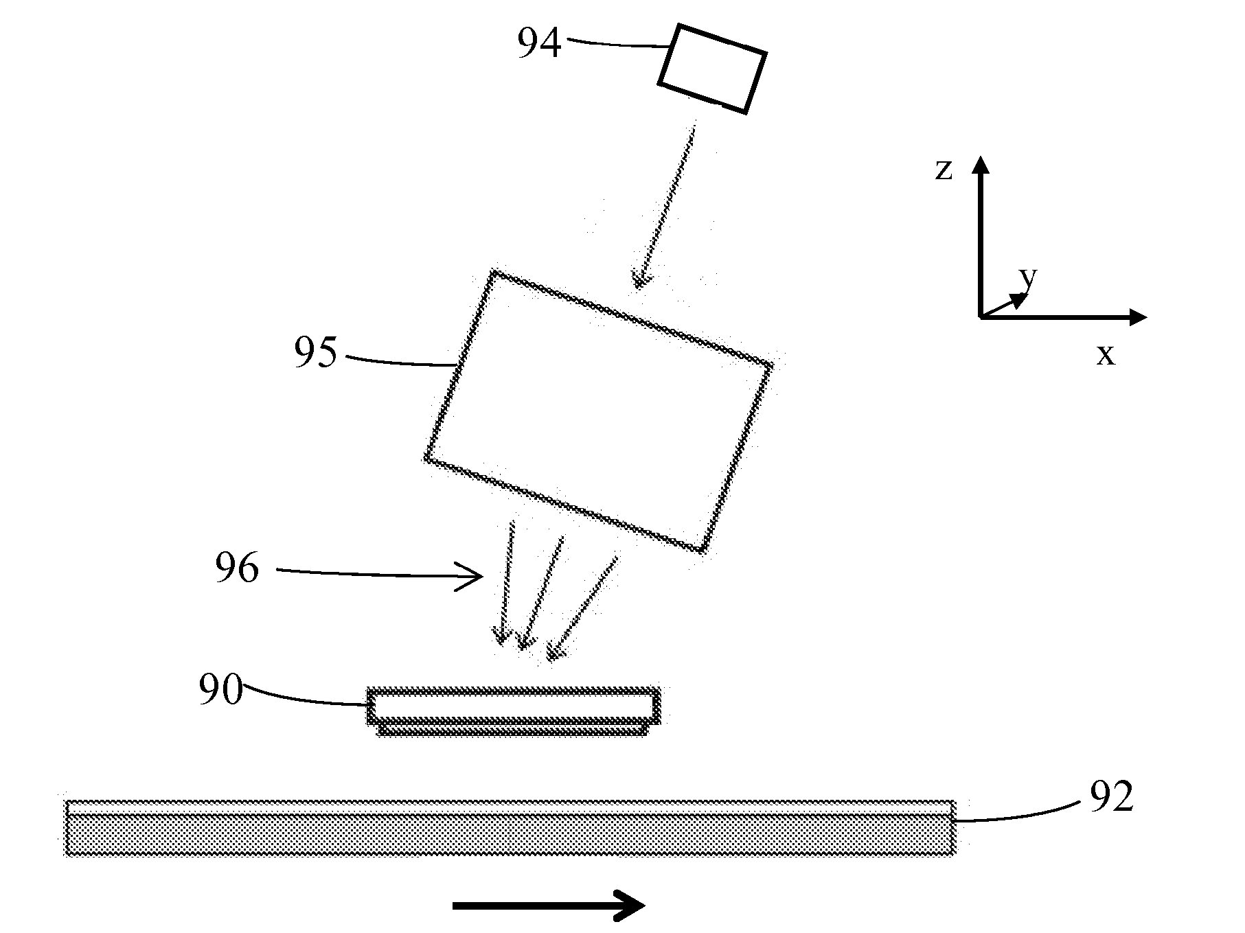
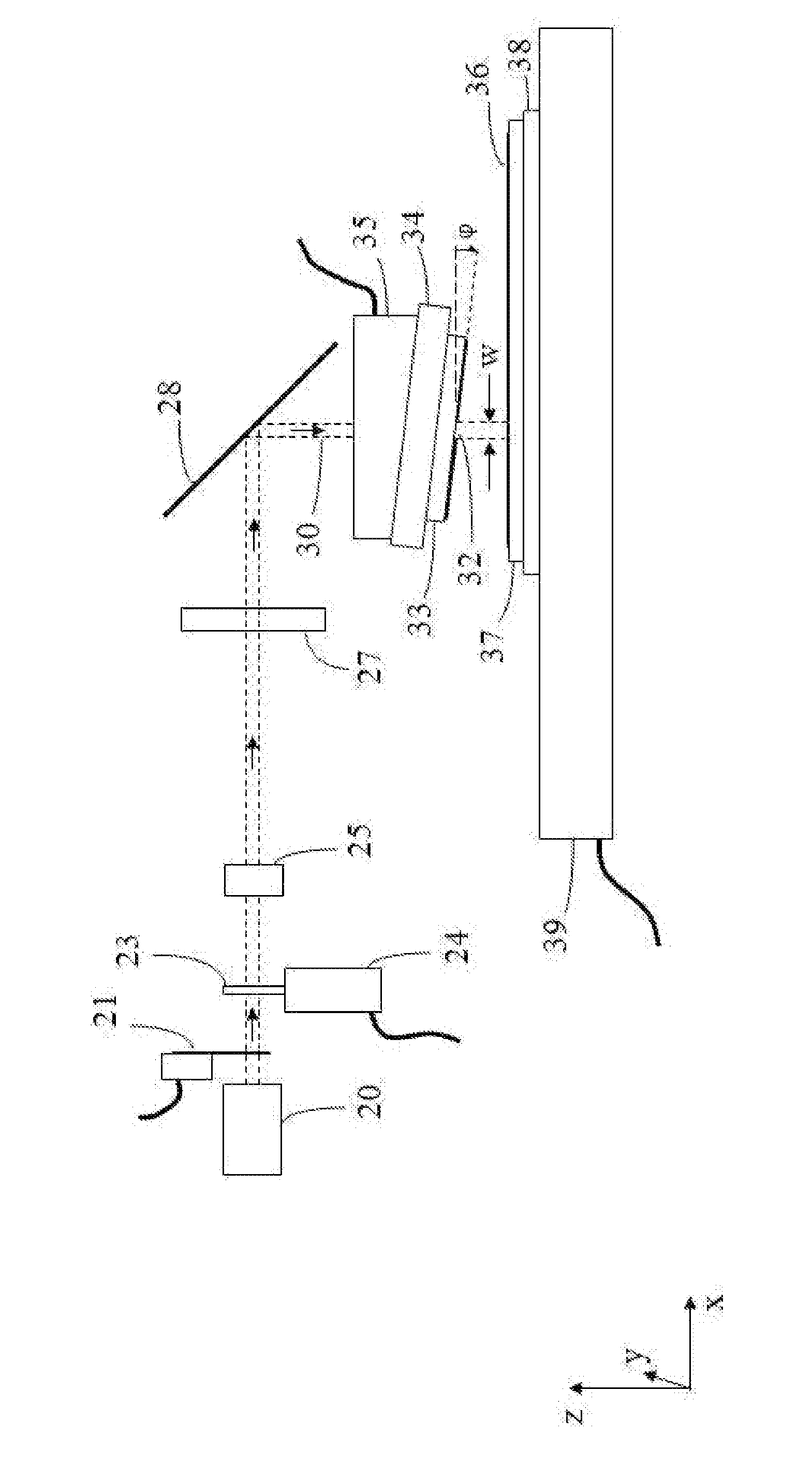
[0047] In the first embodiment of the present invention, refer to figure 1 , the photomask 9 carries a one-dimensional periodic pattern 10 consisting of alternating opaque lines and transparent spaces with a period of 1 μm. The area of ​​pattern 10 is 2mm * 100mm (l x × l y ), and the lines and spaces of pattern 10 are oriented parallel to the xz plane. The mask 9 is fabricated using standard mask fabrication techniques, the lines of the pattern being formed in a layer of chromium on a transparent substrate. The surface of the mask 9 surrounding the pattern 10 is also covered with chrome. The mask 9 is held by a vacuum chuck 12 having a central aperture allowing illumination of the mask pattern 10 by an exposure beam 11 from above. The mask chuck 12 is mounted to a positioning system 13 that includes an actuator that enables the mask 9 to be moved relative to the size 250 mm x 100 mm (L x × L y ) of the larger photoresist-coated substrate 16, which is positioned on the v...


PUM


Abstract

A method and apparatus for printing a pattern of periodic features into a photosensitive layer, including the steps of providing a substrate bearing the layer, providing a mask, arranging the substrate such that it has a tilt angle with respect to the substrate in a first plane orthogonal thereto, providing collimated light for illuminating the mask pattern so as to generate a transmitted light-field composed of a range of transversal intensity distributions between Talbot planes separated by a Talbot distance, and so that said transmitted light-field has an intensity envelope in the first plane, illuminating the mask with said light whilst displacing the substrate relative to the mask in a direction parallel to the first plane and to the substrate, wherein the tilt angle and the intensity envelope are arranged so that the layer is exposed to an average of the range of transversal intensity distributions.

Description

technical field [0001] The present invention generally relates to the field of photolithography for fabricating micro- or nanostructures, and in particular the invention relates to the field of photolithography based on the Taber effect or self-imaging. Background technique [0002] Micro- or nanostructures with feature sizes typically in the range of 10 nm-10 μm are desired for many applications. Such structures should be formed on surfaces whose area varies from a few square millimeters to several square meters. Such applications include flat panel displays and solar panels. [0003] Lithographic techniques for fabricating such structures on large areas have been proposed, for example, nanoimprint lithography using a master and contact photolithography using a roller mask. Nanoimprint lithography requires contact between the mask and the substrate to be printed, and is therefore sensitive to defects since the contact between the master and the substrate degrades the unif...

Claims


Application Information

Patent Timeline
IPC IPC(8): G03F7/20
CPCG03F7/70408G03F7/201G02F1/13G03F7/20G03F7/26
Inventor H.索拉克F.克鲁贝
Owner EULITHA
Why Eureka
Try Eureka