Array substrate, manufacturing method thereof and display device

A technology for an array substrate and a manufacturing method, which is applied in the fields of an array substrate and its manufacturing method, and a display device, and can solve problems such as large leakage current, influence on TFT performance, and insufficient mobility, and achieve stable TFT characteristics, reduced leakage current, and high mobility rate effect

Inactive Publication Date: 2013-11-27
BOE TECH GRP CO LTD
View PDF2 Cites 16 Cited by
  • Summary
  • Abstract
  • Description
  • Claims
  • Application Information

AI Technical Summary

Problems solved by technology

The actual carrier mobility of amorphous silicon TFT is about 10cm 2 / (V*s), but because there are too many defects, most of the charges attracted by the gate electrode are captured in the defects and cannot provide conductivity, so that the equivalent carrier mobility is only less than 1cm 2 / (V*s), cannot meet the needs of large-size display products
[0004] In order to improve the mobility of the active layer, the existing technology uses metal oxide semiconductors to make the active layer, but the mobility of some metal oxide semiconductors is not high enough, and some metal oxide semiconductors have relatively high mobility, but the drain If the current is relatively large, it will affect the performance of the TFT and cause the display to fail to display normally.

Method used


Image

  • Array substrate, manufacturing method thereof and display device
  • Array substrate, manufacturing method thereof and display device
  • Array substrate, manufacturing method thereof and display device

Examples


Embodiment Construction

[0049] In order to make the technical problems, technical solutions and advantages to be solved by the embodiments of the present invention clearer, the following will describe in detail with reference to the drawings and specific embodiments.

[0050] Embodiments of the present invention provide an array substrate, a manufacturing method thereof, and a display device, capable of preparing an active layer with good performance, stability, and high mobility.

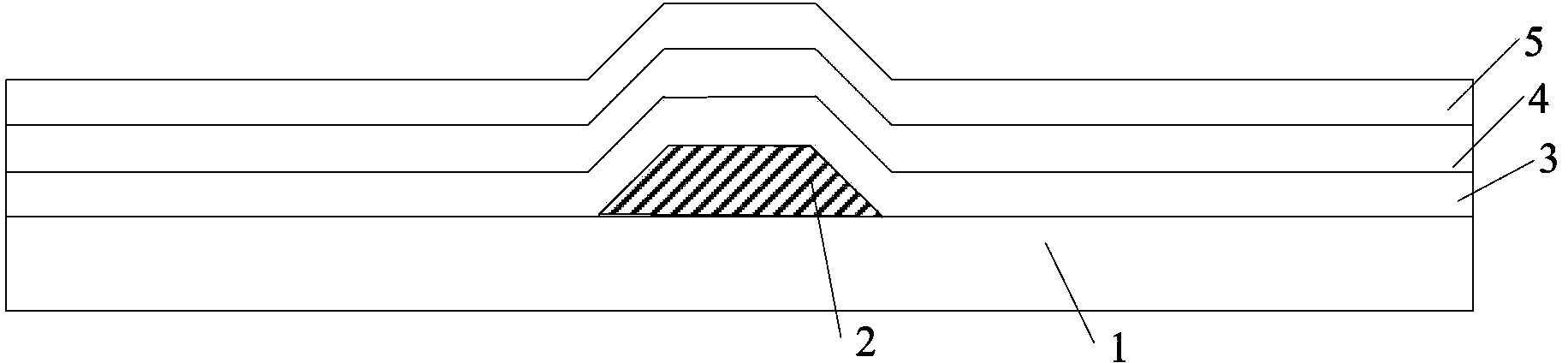
[0051] An embodiment of the present invention provides an array substrate. The active layer of the array substrate is composed of at least two metal oxide semiconductor layers, wherein the mobility of the first metal oxide semiconductor layer close to the gate insulating layer is greater than that close to the source layer. Drain the mobility of the second metal oxide semiconductor layer from the metal layer.

[0052] In the array substrate of the present invention, the first metal oxide semiconductor layer close to the g...


PUM

PropertyMeasurementUnit
thicknessaaaaaaaaaa

Abstract

The invention provides an array substrate, a manufacturing method thereof and a display device, and belongs to the display technical field. An active layer of the array substrate comprises at least two metal-oxide semiconductor layers, wherein the mobility ratio of a first metal-oxide semiconductor layer close to a gate insulation layer is larger than that of a second metal-oxide semiconductor layer close to a source drain metal layer. According to the technical scheme, the active layer which is stable, good in performance and high in mobility ratio can be manufactured.

Description

technical field [0001] The present invention relates to the field of display technology, in particular to an array substrate, a manufacturing method thereof, and a display device. Background technique [0002] With the continuous advancement of technology, users' demand for liquid crystal display equipment is increasing, and TFT-LCD (Thin Film Transistor-Liquid Crystal Display, Thin Film Field Effect Transistor Liquid Crystal Display) has also become the mainstream display used in mobile phones, tablet computers and other products . In addition, with the popularization of display devices, users' demand for large-size display products is becoming more and more common. [0003] The performance of TFT determines the display quality of LCD. Amorphous silicon is often used as the active layer in mass production, but amorphous silicon has many defects and low mobility. The actual carrier mobility of amorphous silicon TFT is about 10cm 2 / (V*s), but because there are too many d...

Claims


Application Information

Patent Timeline
Patent Type & Authority Applications(China)
IPC IPC(8): G02F1/1362G02F1/1368H01L27/12H01L21/77
CPCH01L27/1225H01L27/127H01L27/1288H01L29/66969H01L29/7869H01L29/78696
Inventor 闫梁臣
Owner BOE TECH GRP CO LTD
Why Eureka
Try Eureka