Multichannel RAM (random-access memory) reading/writing circuit and method

A multi-channel, circuit technology, applied in the field of multi-channel read/write RAM circuits, can solve the problems of bus arbitration, complex decoding mechanism, and increased system design complexity, and achieve increased average power consumption, improved access bandwidth, and easy access. effect achieved

Active Publication Date: 2013-12-04
NATIONZ TECH INC
View PDF5 Cites 7 Cited by
  • Summary
  • Abstract
  • Description
  • Claims
  • Application Information

AI Technical Summary

Problems solved by technology

From the perspective of improving RAM access bandwidth, it is very convenient to use the AHB bus, but its bus arbitration and decoding mechanisms are relatively complicated. In some small systems, the use of the AHB bus will increase the design complexity of the entire system.

Method used


Image

  • Multichannel RAM (random-access memory) reading/writing circuit and method
  • Multichannel RAM (random-access memory) reading/writing circuit and method
  • Multichannel RAM (random-access memory) reading/writing circuit and method

Examples


Embodiment Construction

[0031] In order to make the technical solutions and advantages of the present invention clearer, the present invention will be further described in detail below through specific embodiments in conjunction with the accompanying drawings.

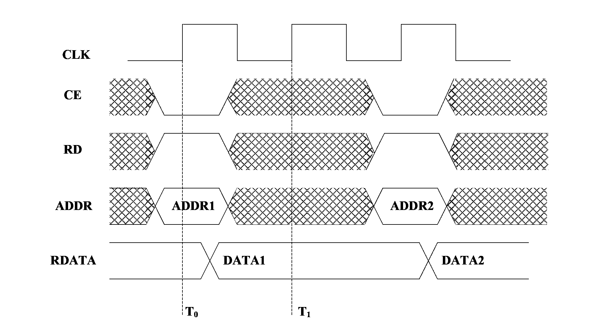
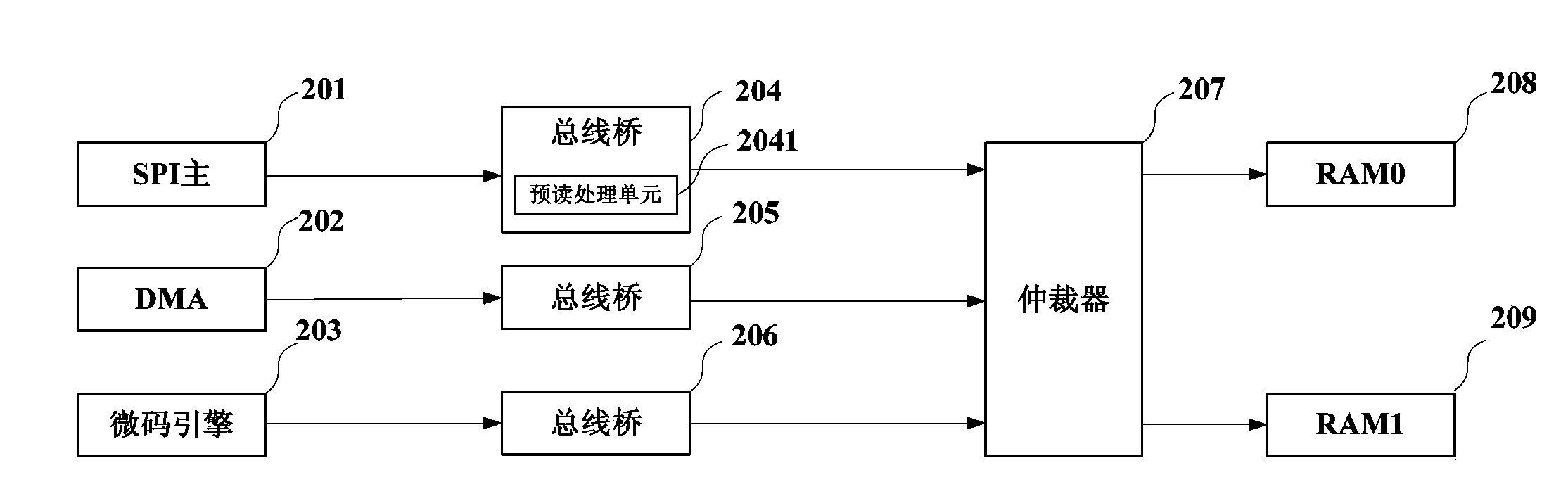
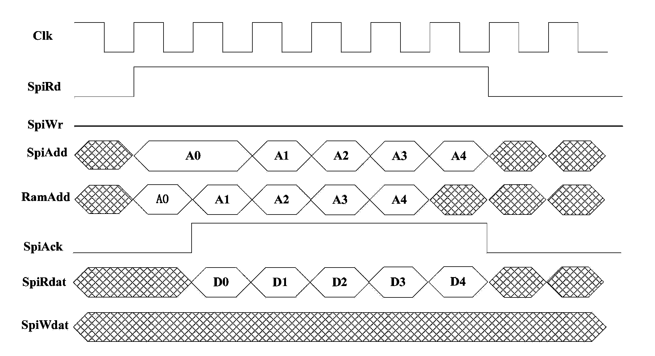
[0032] In this application, the general idea of ​​the invention is: in order to improve RAM access bandwidth, multiple RAMs are provided in the circuit, and multiple RAMs can simultaneously accept read / write operations from multiple Masters on the bus. The specific implementation method is as follows:

[0033] The present invention provides a multi-channel read / write RAM circuit, which includes at least two master devices, at least two bus bridges, arbitrators and at least two RAMs; wherein, each master device is connected to the arbitrator through a bus bridge , at least two RAMs are connected to the arbiter.

[0034] Master is used to issue the system bus signal for reading / writing RAM, and pass it to the bus bridge for conversion.

[003...


PUM


Abstract

The invention provides a multichannel RAM (random-access memory) reading/writing circuit and method. A plurality of RAMs are added in the circuit, a bus bridge, an arbiter and multiplexer cooperates, simpler circuit control logic is used to allow access bandwidth of RAM is increased greatly while system clock frequency is unchanged, and average system power consumption is unchanged. The multichannel RAM reading/writing circuit is simple, low in cost and easy to implement in a system.

Description

technical field [0001] The invention relates to the technical field of storage, in particular to a multi-channel read / write RAM circuit and method. Background technique [0002] At present, chips based on SoC (System on Chip, system-on-chip) architecture have been widely used in various electronic systems. On-chip RAM (Radom Access Memory, Random Access Memory) is an important part of the SoC system. It is generally used as instruction memory, data exchange space and temporary data storage space. The speed of each master device (Master) on the bus to access RAM becomes A key factor restricting system performance. The read / write operation of RAM under most current technologies must be delayed by one beat, that is, when doing read / write operations, the read / write data must always be valid in the next beat when the read signal is valid. Please refer to figure 1 , taking reading RAM as an example, CE in the figure is the enable signal of RAM, which is active at low level, and...

Claims


Application Information

Patent Timeline
Patent Type & Authority Applications(China)
IPC IPC(8): G06F3/06
Inventor 唐端午
Owner NATIONZ TECH INC
Why Eureka
Try Eureka