Transparent conductive film, substrate with transparent conductive film, and method for manufacturing same

A technology of transparent conductive film and transparent substrate, which can be used in the removal of conductive materials by light, printed circuit manufacturing, cable/conductor manufacturing, etc.

Inactive Publication Date: 2013-12-18
PANASONIC CORP
View PDF9 Cites 10 Cited by
  • Summary
  • Abstract
  • Description
  • Claims
  • Application Information

AI Technical Summary

Problems solved by technology

[0003] However, this approach may result in a level difference corresponding to the film thickness of the conductive region 4 with respect to the surface of the transparent substrate 9, such as by Figure 3B indicated by the double-headed arrow in the

Method used


Image

  • Transparent conductive film, substrate with transparent conductive film, and method for manufacturing same
  • Transparent conductive film, substrate with transparent conductive film, and method for manufacturing same
  • Transparent conductive film, substrate with transparent conductive film, and method for manufacturing same

Examples


Embodiment 1

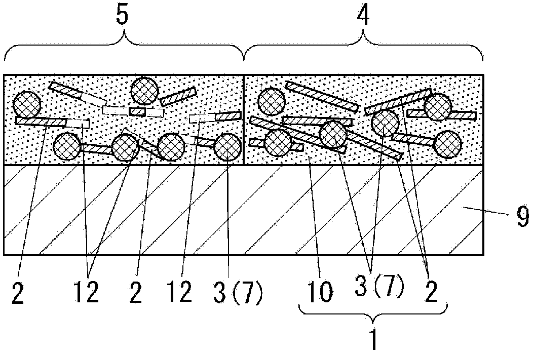
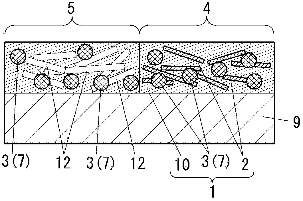
[0094] The transparent substrate 9 used was a non-alkali glass plate ("No. 1737", refractive index at a wavelength of 500 nm: 1.50 to 1.53, available from Corning Inc.). The transparent conductive material A was applied on the surface of the transparent substrate by spin coating and heated under the conditions of 100° C. and 5 minutes for drying and hardening to give a transparent conductive film having a film thickness of 100 nm. After that, in order to form the insulating region, there will be 0.5J / cm 2 The light of the average energy density is emitted to the left half of the transparent conductive film by means of a UV-YAG laser. Thus, a substrate with a transparent conductive film having a conductive region in the right half of the transparent conductive film and an insulating region in the left half thereof was prepared.

Embodiment 2

[0096] A transparent conductive film having a film thickness of 100 nm was prepared in a similar manner to Example 1 except that transparent conductive material A was replaced with transparent conductive material B. After that, an insulating region was formed similarly to Example 1 to give a substrate with a transparent conductive film having a conductive region in the right half of the transparent conductive film and an insulating region in the left half thereof.

Embodiment 3

[0098] A transparent conductive film having a film thickness of 100 nm was prepared in a similar manner to Example 1 except that transparent conductive material A was replaced with transparent conductive material C. After that, an insulating region was formed similarly to Example 1 to give a substrate with a transparent conductive film having a conductive region in the right half of the transparent conductive film and an insulating region in the left half thereof.


PUM

PropertyMeasurementUnit
diameteraaaaaaaaaa
lengthaaaaaaaaaa
particle sizeaaaaaaaaaa

Abstract

Provided is a transparent conductive film that is capable of converting a conductive portion to an insulating portion more easily and more quickly than in the past, and also capable of reducing the step between the conductive portion and the insulating portion. A conductive portion (4) and an insulating portion (5) are formed. The conductive portion (4) contains a resin component (10), a metallic nanowire (2), and an insulating reinforcement component (3). The insulating reinforcement component (3) is a nanoparticle with higher light absorbency than the metallic nanowire (2). The insulating portion (5) contains either a resin component (10) and no metallic nanowire (2), or a resin component (10) and a metallic nanowire (2) with a smaller aspect ratio than the abovementioned metallic nanowire (2).

Description

technical field [0001] The invention relates to a transparent conductive film used in various devices including a touch screen, a base material with the transparent conductive film, and a preparation method thereof. Background technique [0002] Transparent conductive films are widely used in touch screens, organic EL devices, liquid crystal displays, solar cells, and other devices. For example, an ITO film as a transparent conductive film is formed on the surface of a transparent substrate by sputtering, and a transparent electrode is produced by patterning (patterning) on ​​the ITO film by photolithography. In addition if Figure 3A As shown in , a transparent conductive film 1 containing metal nanowires 2 is formed on the surface of a transparent substrate 9, and its unwanted area is removed by photolithography or laser beam processing to produce a conductive area that is preserved by 4 composed of transparent electrodes, such as Figure 3B shown in . In addition, if ...

Claims


Application Information

Patent Timeline
Patent Type & Authority Applications(China)
IPC IPC(8): H01B5/14H01B13/00
CPCB82Y30/00G06F3/041G06F2203/04103C09D101/02H05K1/0274H05K1/0313H05K1/097H05K3/027H05K3/4664H05K2201/032H05K2201/2054
Inventor 辻本光忠政明彦松井太佑安原绘理
Owner PANASONIC CORP
Why Eureka
Try Eureka