Interconnection structure and its formation method

An interconnection structure, metal layer technology, applied in electrical components, electrical solid devices, circuits, etc., can solve the problems of time-dependent dielectric breakdown effect is not obvious, metal atoms are unstable, etc., to avoid performance degradation or failure, improve The effect of electrical properties

Active Publication Date: 2013-12-25
SEMICON MFG INT (SHANGHAI) CORP
View PDF3 Cites 13 Cited by
  • Summary
  • Abstract
  • Description
  • Claims
  • Application Information

AI Technical Summary

Problems solved by technology

However, using N 2 or H 2 The principle of plasma reduction is based on the fact that the plasma is ionized under high pressure into ion atoms, etc., and the reduction reaction occurs with the surface of the copper interconnection line, and CuO is reduced to Cu, but the metal atoms are still in an unstable state, which is very important for suppressing the loss of copper ions, And the effect of improving time-related dielectric breakdown is not obvious

Method used


Image

  • Interconnection structure and its formation method
  • Interconnection structure and its formation method
  • Interconnection structure and its formation method

Examples


Embodiment Construction

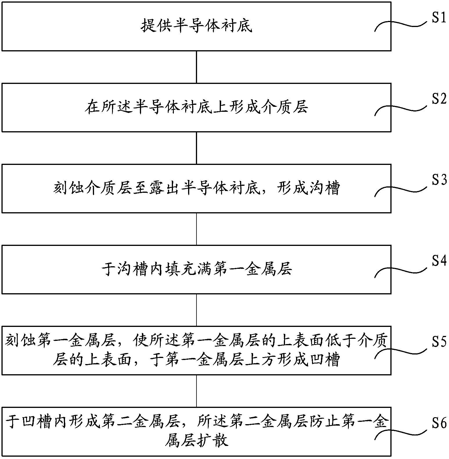
[0032] In order to make the above objects, features and advantages of the present invention more comprehensible, specific implementations of the present invention will be described in detail below in conjunction with the accompanying drawings.

[0033] In the following description, many specific details are set forth in order to fully understand the present invention, but the present invention can also be implemented in other ways than those described here, so the present invention is not limited by the specific embodiments disclosed below.

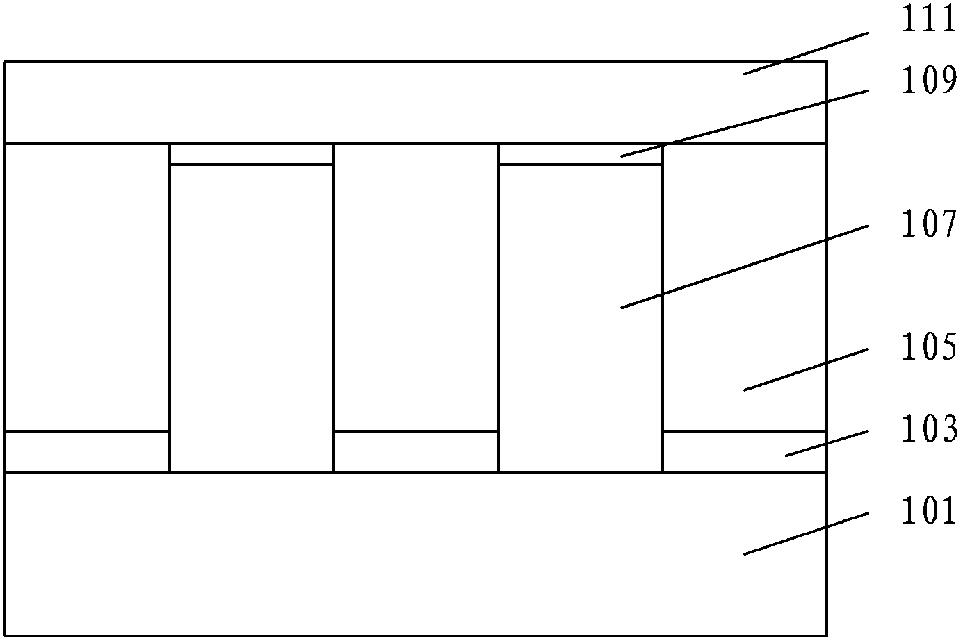
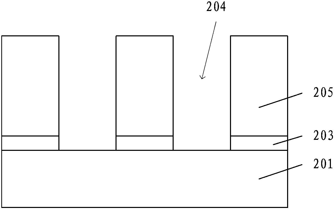
[0034] As mentioned in the background technology section, in the interconnection structure formed in the prior art, copper atoms in the metal layer are prone to electromigration, resulting in the formation of hillocks in some areas of the metal layer due to the accumulation of copper atoms or the formation of voids due to the migration of copper atoms , resulting in performance degradation or even failure of the interconnect structure. An...


PUM

PropertyMeasurementUnit
thicknessaaaaaaaaaa
thicknessaaaaaaaaaa

Abstract

An interconnection structure and its formation method are disclosed. The interconnection structure comprises a semiconductor substrate, a dielectric layer positioned on the semiconductor substrate, a first metal layer positioned on the semiconductor substrate and a second metal layer positioned, wherein the first metal layer is positioned in the dielectric layer, the upper surface of the first metal layer is lower than the upper surface of the dielectric layer, and a groove is arranged above the first metal layer. The interconnection structure also comprises a second metal layer which is positioned in the groove and is used for preventing diffusion of the first metal layer. According to the interconnection structure and its formation method, the second metal layer is deposited on the surface of the first metal layer positioned in the dielectric layer so as to prevent electromigration of atoms in the first metal layer. And then, the interconnection structure performance degradation or failure caused by electromigration of atoms in the first metal layer is avoided, and electrical properties of the formed interconnection structure are raised.

Description

technical field [0001] The invention relates to the technical field of semiconductor manufacturing, in particular to an interconnection structure and a forming method thereof. Background technique [0002] In the existing semiconductor process, aluminum is usually used as the material of the interconnection structure; however, because copper has higher electrical conductivity and better anti-electromigration characteristics, copper gradually replaces aluminum and is widely used in VLSI in the interconnection line. However, in the process of using copper as an interconnection line, it is found that copper is easy to diffuse rapidly in the dielectric layer, which may cause high leakage current and breakdown of the dielectric layer. Provides a barrier layer that prevents copper diffusion. [0003] With the development of VLSI, especially the continuous reduction in the size of high-performance logic devices, the barrier layer cannot completely prevent copper from diffusing fr...

Claims


Application Information

Patent Timeline
Patent Type & Authority Applications(China)
IPC IPC(8): H01L23/528H01L21/768
Inventor 周鸣
Owner SEMICON MFG INT (SHANGHAI) CORP
Why Eureka
Try Eureka