Method for inhibiting copper electromigration in hybrid bonding of wafers

A technology of hybrid bond and copper electricity, which is applied in the manufacture of circuits, electrical components, semiconductors/solid-state devices, etc., can solve the problems that copper cannot be effectively interconnected and reduce the stability of electrical connection of finished products, so as to increase contact resistance, inhibit thermal expansion, and reduce The effect of the height of the sag

Active Publication Date: 2018-05-04
YANGTZE MEMORY TECH CO LTD
View PDF6 Cites 6 Cited by
  • Summary
  • Abstract
  • Description
  • Claims
  • Application Information

AI Technical Summary

Problems solved by technology

Using the above method has the following defects: before annealing, there are depressions produced in the chemical mechanical polishing process in the metal layer, and the above depressions cannot be completely filled after the copper

Method used


Image

  • Method for inhibiting copper electromigration in hybrid bonding of wafers
  • Method for inhibiting copper electromigration in hybrid bonding of wafers
  • Method for inhibiting copper electromigration in hybrid bonding of wafers

Examples


Embodiment Construction

[0016] The specific embodiments of the present invention will be described in detail below in conjunction with the accompanying drawings, but it should be understood that the protection scope of the present invention is not limited by the specific embodiments.

[0017] Unless expressly stated otherwise, throughout the specification and claims, the term "comprise" or variations thereof such as "includes" or "includes" and the like will be understood to include the stated elements or constituents, and not Other elements or other components are not excluded.

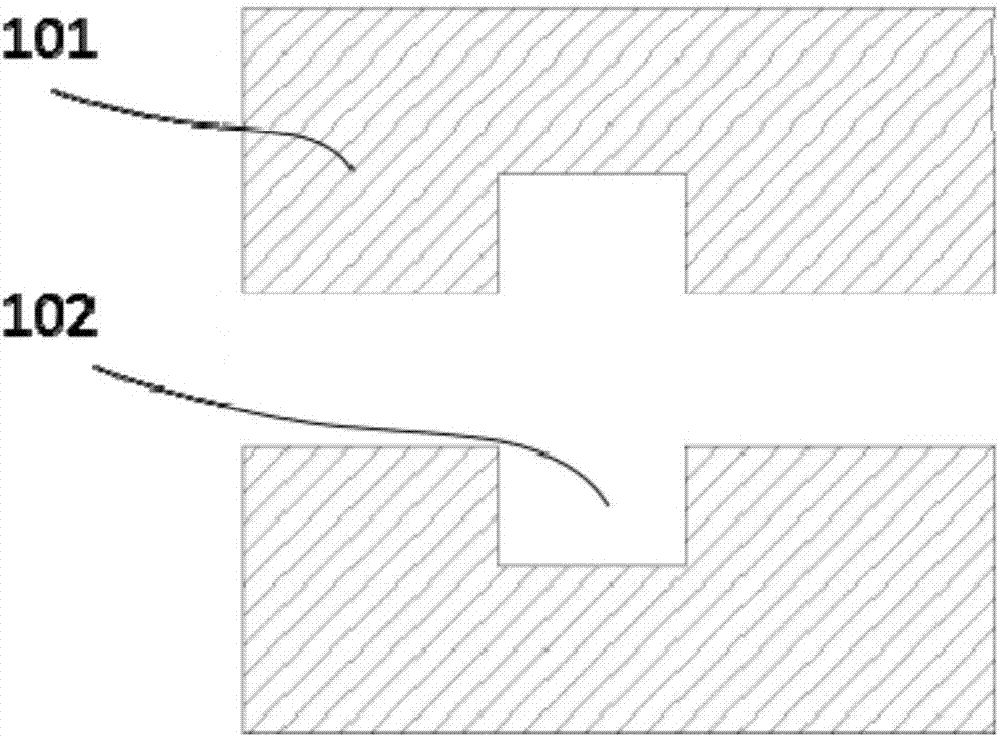
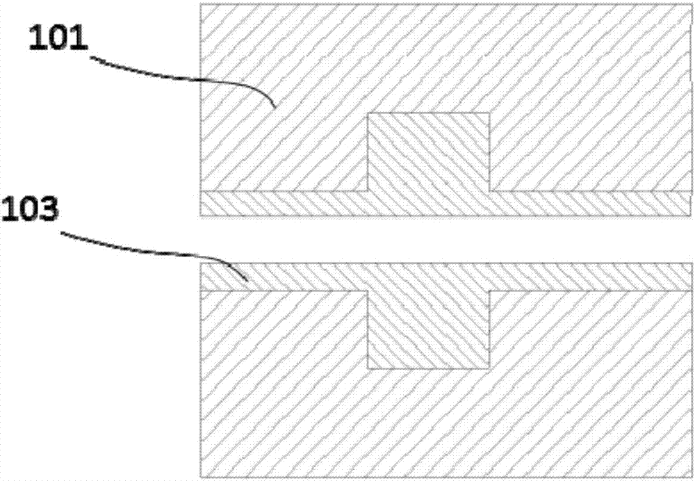
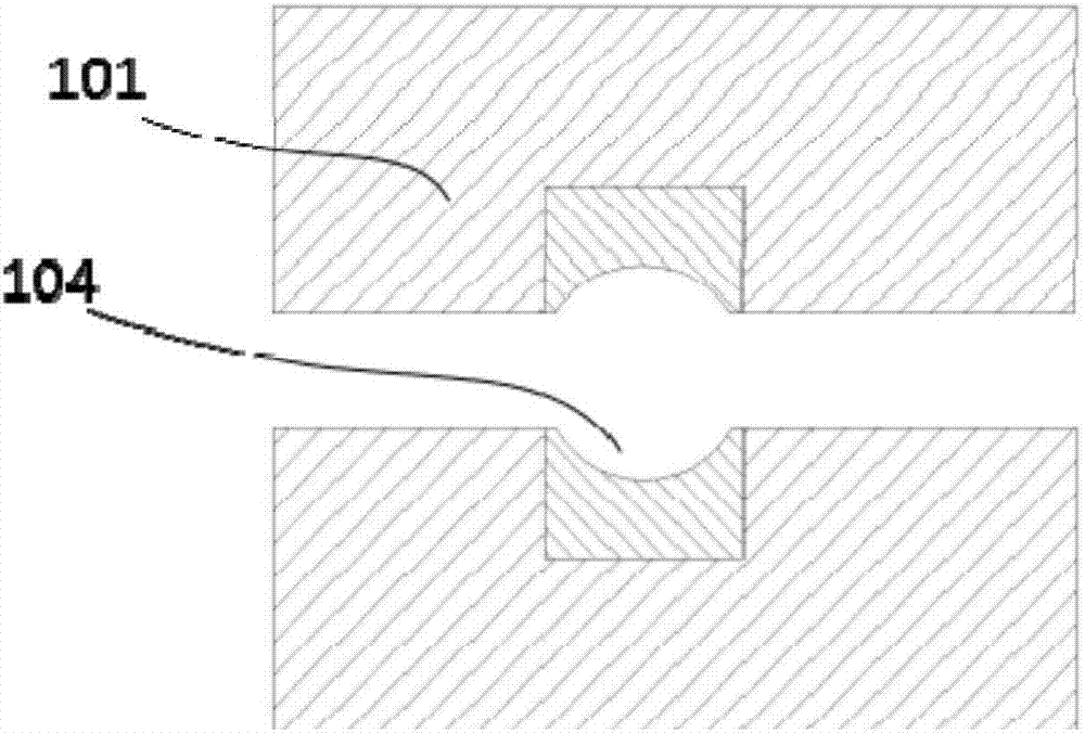
[0018] The following firstly introduces the wafer bonding method in the prior art, which provides a strong connection at the interface between two substrates. The substrate is a semiconductor substrate, and the substrate may also be a semiconductor wafer. The substrate may comprise a donor wafer providing metal connections and via connections, this donor wafer may be bonded to another device wafer, and the substrate of the...


PUM

PropertyMeasurementUnit
Thicknessaaaaaaaaaa

Abstract

The invention discloses a method for inhibiting copper electromigration in hybrid bonding of wafers. The method comprises the following steps of forming metal layers on at least two semiconductor substrates; carrying out chemico-mechanical polishing on the semiconductor substrates to form a plurality of recesses in the metal layers; plating the metal layers with the plurality of recesses with graphene; and carrying out thermal treatment on the at least two semiconductor substrates to bond the metal layers through the graphene. The recesses of specific heights are firstly formed through control, single-layer graphene is accurately transferred into each recess to form a cover coating, wafer bonding is carried out through a hybrid bonding method of the wafers, and thermal treatment is finallycarried out at certain temperature, so that copper electromigration can be inhibited.

Description

technical field [0001] The invention relates to a wafer hybrid bonding method, in particular to a method for suppressing copper electromigration in wafer hybrid bonding. Background technique [0002] New improvements for wafer bonding are increasingly important in 3D IC construction. In wafer bonding, two semiconductor wafers are bonded together to form a three-dimensional stack without the need for intervening substrates or devices. In applications requiring two different wafer types, this approach can provide a single device with two functional devices in one package. In one specific application, a CMOS image sensor, a substrate including an image sensor array, can be bonded onto a circuit wafer to provide a 3D IC that includes all the circuitry needed to implement the image sensor in the same circuit board area as the sensor array system that provides a complete image sensing solution in a single packaged integrated circuit device. [0003] Previously known wafer bondi...

Claims


Application Information

Patent Timeline
IPC IPC(8): H01L21/18H01L21/306H01L21/324
CPCH01L21/187H01L21/30625H01L21/324
Inventor 丁滔滔王家文汪小军李春龙郭帅邢瑞远曾凡志
Owner YANGTZE MEMORY TECH CO LTD
Why Eureka
Try Eureka