Terminal structure of chiplike electric component

a technology of terminal structure and electric component, which is applied in the direction of resistor details, resistive material coating, fixed capacitor details, etc., can solve the problems of difficult to completely block the entry of electromigration-causing factors, the resistance value of the surface electrode b>3/b> reaches, and the electromigration arises

Inactive Publication Date: 2009-09-17
HOKURIKU ELECTRIC INDS
View PDF8 Cites 9 Cited by
  • Summary
  • Abstract
  • Description
  • Claims
  • Application Information

AI Technical Summary

Benefits of technology

[0029]When the glass layer is provided to completely cover the surface of the electrical element forming layer as well as the surface of the end portion of the electrical element forming layer and also to partially cover the front electrode, and the insulating resin layer is provided to completely cover the surface of the glass layer as well as the surface of the end portion of the glass layer, and also to partially cover the front electrode as described above, the surface of the end portion of the electrical element forming layer is entirely covered with the glass layer. Then, the entire surface of the glass layer, which covers the surface of the end portion of the electrical element forming layer, is covered with the insulating resin layer. Accordingly, even if electromigration-causing factors have entered into the insulating resin layer in the vicinity of the peak of a raised portion of the electrical element forming layer, the glass layer is present under the insulating resin layer. Entry of the electromigration-causing factors may be thereby blocked. Consequently, according to the present invention, entry of the electromigration-causing factors into front electrode through the insulating resin layer in the vicinity of the peak of the raised portion of the electrical element forming layer may be sufficiently blocked. Further, the overlap length between the insulating resin layer and the conductive layer, as measured in the arrangement direction of the front electrode and the electrical element forming layer is defined to block electromigration whereby silver contained in the front electrode migrates along the interface between the insulating resin layer and the conductive layer, and separates out from the boundary portion between the conductive thin film layer and the insulating resin layer. With this arrangement, it may be possible to sufficiently block migration of the silver contained in the front electrode along the interface between the insulating resin layer and the conductive layer and then separating-out of the silver after coming out from the boundary portion between the conductive thin film layer and the insulating resin layer due to the electromigration.
[0030]The present invention may be applied to a terminal structure of a trimmable chip-like electric component as well. In this terminal structure, in order to allow laser trimming to be performed on an electrical element forming layer after the chip-like electric component has been mounted onto a circuit board, a glass layer is not entirely covered with an insulating resin layer. The insulating resin layer is provided to cover the surface of an end portion of the glass layer and to partially cover the surface of a front electrode. Even in the terminal structure of the trimmable chip-like electric component as described above, an overlap length between the insulating resin layer and a conductive layer, as measured in an arrangement direction of the front electrodes and the electrical element forming layer, is defined so that silver contained in the front electrode is prevented from migrating along an interface between the insulating resin layer and the conductive layer and then being separated out from a boundary portion between a conductive thin film layer and the insulating resin layer.

Problems solved by technology

However, it is known that when an electric apparatus including a circuit board with the chip-like electric component having this terminal structure mounted thereon is placed in an atmosphere rich in a sulfur component for a long time of period, a problem with electromigration arises.
For this reason, it is considered difficult to completely block entry of electromigration-causing factors (e.g. moisture and sulfur).
Accordingly, a resistance value of the front electrode 3 is increased, which finally causes a problem that the resistance value of the surface electrode 3 reaches to an open level at which disconnection occurs.

Method used


Image

  • Terminal structure of chiplike electric component
  • Terminal structure of chiplike electric component
  • Terminal structure of chiplike electric component

Examples


Embodiment Construction

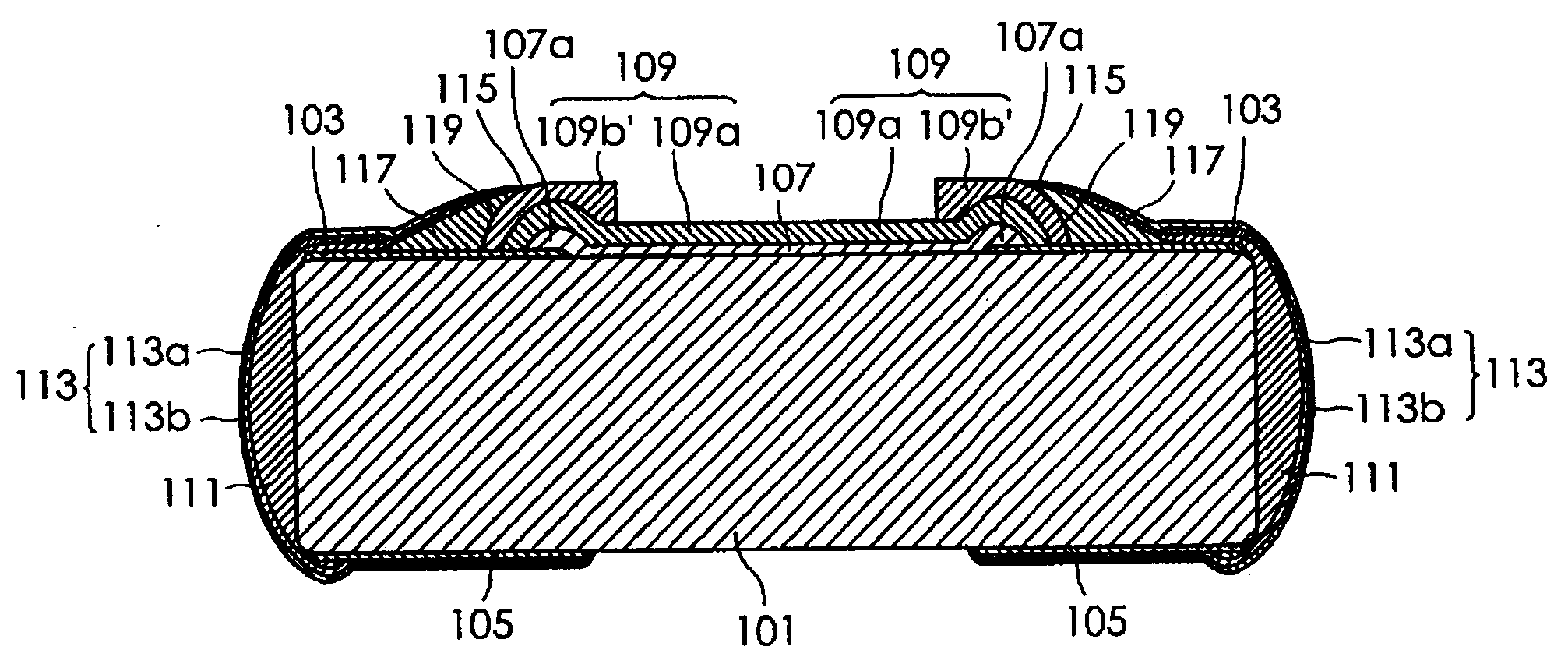
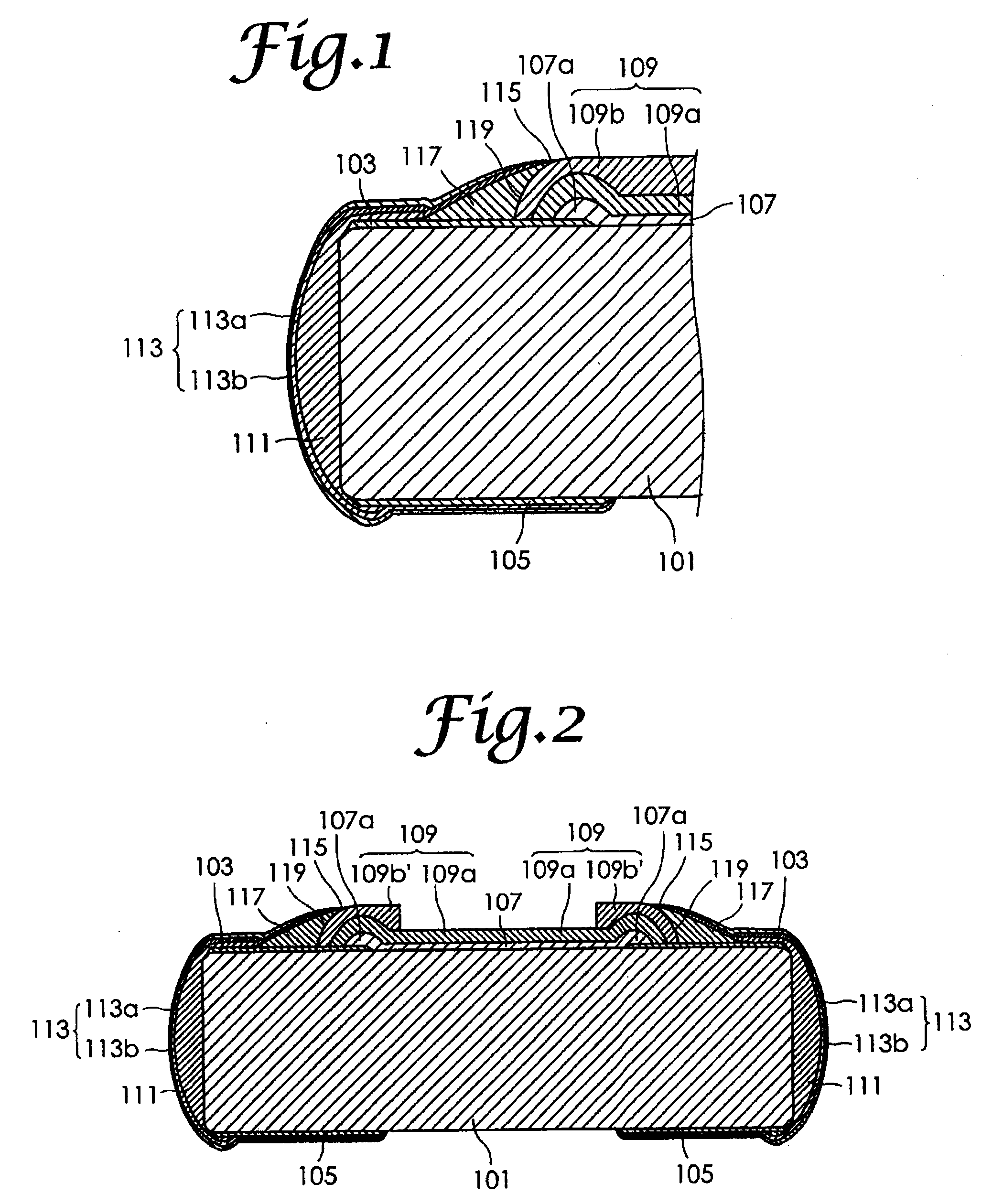
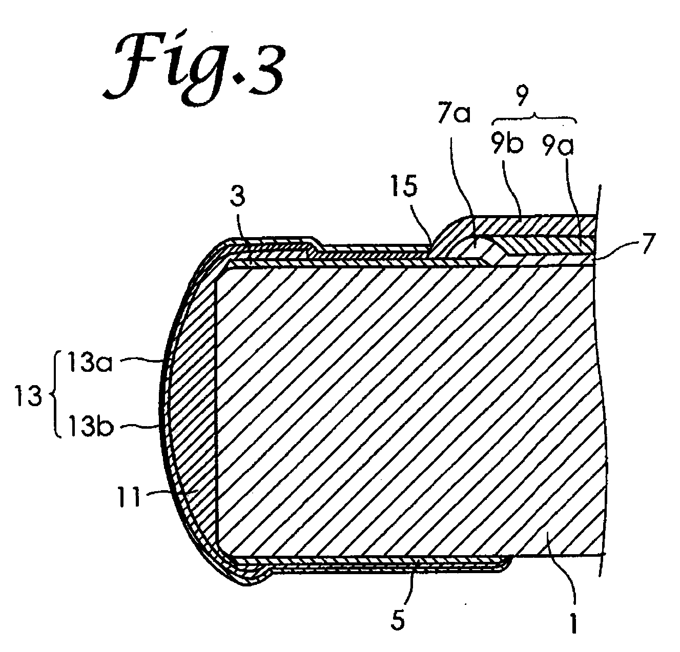
[0043]An example of a terminal structure of a chip-like electric component according to the present invention will be described in detail with reference to a vertically sectional view shown in FIG. 1 wherein the terminal structure according to the present invention is applied to a terminal structure of a chip-like resistor. Reference numerals obtained by adding 100 to reference numerals used in FIG. 3 are assigned to components corresponding to those in FIG. 3 described before, for illustration.

[0044]In the terminal structure of the chip-like resistor in this embodiment, a metal-glaze-based surface electrode 103 and a metal-glaze-based back electrode 105 both containing silver are respectively provided on a front surface and a back surface of an insulating ceramic substrate 101. These metal-glaze-based front electrode 103 and metal-glaze-based back electrode 105 both containing silver are respectively formed by forming an electrode pattern on the insulating ceramic substrate by mean...


PUM

PropertyMeasurementUnit
viscosityaaaaaaaaaa
sizeaaaaaaaaaa
particle sizeaaaaaaaaaa

Abstract

A terminal structure of a chip-like electric component capable of blocking entry of electromigration-causing factors through an insulating resin layer in the vicinity of the peak of a raised portion of an electrical element forming layer is obtained. A metal-glaze-based front electrode 103 containing silver is provided on a surface of an insulating ceramic substrate 101. A resistor layer 107 electrically connected to the front electrode 103 is provided on the substrate surface. A glass layer 109a is provided to completely cover a surface of the resistor layer 107 as well as a surface of an end portion of the resistor layer 107 and also to partially cover the front electrode 103. An insulating resin layer 109b is provided to cover a surface of the glass layer 109a as well as a surface of at least an end portion of the glass layer 109a and to partially cover the front electrode 103. A conductive layer 117 made of a resin-based conductive paint is provided to extend over the surface of the front electrode 103 and an portion of the insulating resin layer 109b in the vicinity of the peak of raised end portion of the insulating resin layer 109b. The resin-based conductive paint is made by kneading particulate conductive silver powder and scale-like conductive silver powder into an epoxy-based insulating resin paint.

Description

TECHNICAL FIELD[0001]The present invention relates to a terminal structure of a chip-like electric component.BACKGROUND ART[0002]Chip-like electric components typically include a chip resistor, a chip inductor, a chip capacitor, and a chip-like composite electronic component formed by a combination of a plurality of types of electrical elements. Among the chip-like electric components are a chip-like electric component referred to as a multiple chip component of a multiple structure with a plurality of electrodes provided respectively on two opposed sides of an insulating substrate, in addition to a chip-like electric component having an electrode for soldering at each end of an insulating substrate.[0003]Among terminal structures adopted in the conventional chip-like electric components, there is a terminal structure that uses a metal-glaze-based electrode containing silver. A configuration example of the terminal structure of this type will be described with reference to a termina...

Claims


Application Information

Patent Timeline
Patent Type & Authority Applications(United States)
IPC IPC(8): H01C1/012
CPCH01C1/012H01C1/142H01C17/006H01C7/003H01C1/148H01C7/00H01C17/06H01G4/06H01G4/252
Inventor NOMURA, YUTAKATAKEUCHI, KATSUMI
Owner HOKURIKU ELECTRIC INDS
Why Eureka
Try Eureka