Method for manufacturing holographic moulded plate
A manufacturing method and technology of embossing plates, applied in the directions of plate preparation and printing, can solve the problems of high development cost and equipment dependence, achieve strong anti-counterfeiting function, reduce plate-making costs, and achieve the effect of three-dimensional printing effect.
- Summary
- Abstract
- Description
- Claims
- Application Information
AI Technical Summary
Problems solved by technology
Method used
Image
Examples
Embodiment 1
[0036] The manufacturing method of this holographic embossed plate, the manufacturing method of this holographic embossed plate, comprises the following steps:
[0037] (1) Electroforming is used to form a molded nickel plate;
[0038] (2) Set a fine adjustment area on the molded nickel plate, divide each pixel in the fine adjustment area into multiple sub-pixels, and each sub-pixel contains multiple segments of molded stripes;
[0039] (3) Using laser ablation to reduce the height of some or all of the embossed stripes in the sub-pixels to form the shape of patterns or characters.
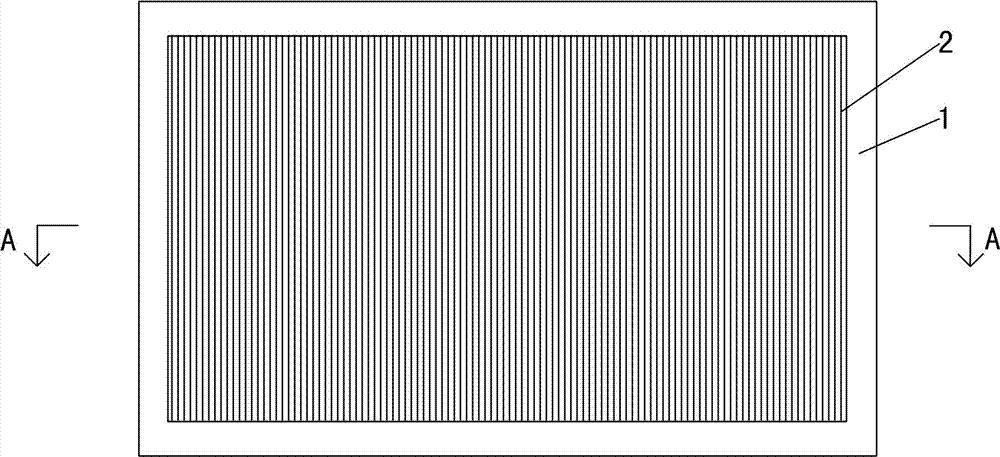
[0040] Through the above manufacturing method, forming such as Figures 1 to 8 Holographic stamped version shown.
[0041] like figure 1 and figure 2 As shown, this holographic molded plate includes a molded nickel plate 1, and a plurality of molded stripes 2 are arranged on the molded nickel plate 1, and the height of the molded stripes 2 is 0.01 mm; image 3 As shown, the molded nickel pla...
Embodiment 2
[0048] The manufacturing method of this holographic embossed plate comprises the following steps:
[0049] (1) Electroforming is used to form a molded nickel plate;
[0050] (2) First coat the photosensitive resin layer on the molded nickel plate, and then form a fine adjustment area by exposure and development;
[0051] (3) Reduce the height of some or all of the embossed stripes in the fine adjustment area by corrosion to form the shape of patterns or characters.
Embodiment 3
[0053] The manufacturing method of this holographic embossed plate comprises the following steps:
[0054] (1) Electroforming is used to form a molded substrate opposite to the pattern of the molded nickel plate;
[0055] (2) Coating a photosensitive resin layer on the molded substrate;
[0056] (3) On the photosensitive resin layer, a temporary adjustment area opposite to the grain of the fine adjustment area is formed by exposure and development;
[0057] (4) Perform the first electroforming on the temporary adjustment area to form a fine adjustment area;
[0058] (5) Cleaning off the photosensitive resin layer on the molded substrate;
[0059] (6) Perform the second electroforming on the molded substrate to form other parts of the molded nickel plate, and complete the production of the whole holographic molded plate.
PUM
| Property | Measurement | Unit |
|---|---|---|
| height | aaaaa | aaaaa |
| area | aaaaa | aaaaa |
Abstract
Description
Claims
Application Information


