Array substrate and liquid crystal display device
An array substrate and grid line technology, applied in nonlinear optics, instruments, optics, etc., can solve problems such as poor friction of alignment films, and achieve the effect of reducing resistance and reducing production rate
- Summary
- Abstract
- Description
- Claims
- Application Information
AI Technical Summary
Problems solved by technology
Method used
Image

Examples
Embodiment 1
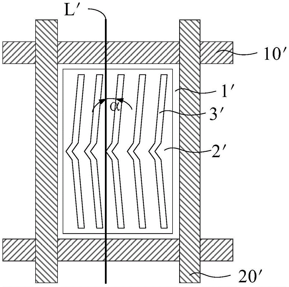
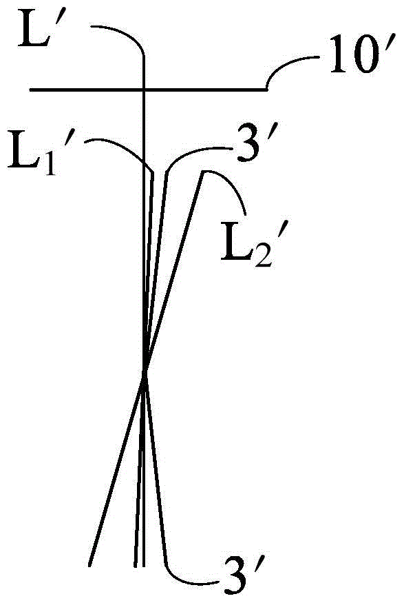
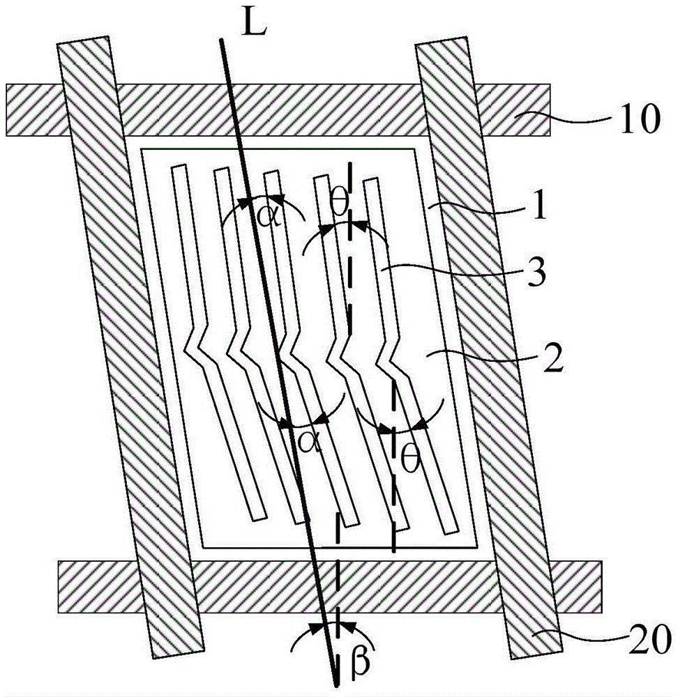
[0018] combine image 3 and Figure 4 As shown, the embodiment of the present invention provides an array substrate, which includes a substrate 100 , gate lines 10 and data lines 20 formed on the substrate 100 , and pixel units 1 defined by the gate lines 10 and data lines 20 . Wherein, the pixel unit 1 includes a TFT (not shown in the figure), a common electrode 4 and a pixel electrode 2 . TFT is used as a switching device, its gate electrode is connected to the gate line 10, its source electrode is connected to the data line 20, and its drain electrode is connected to the pixel electrode 2, which is used to control and generate an electric field that drives the deflection of liquid crystal molecules. An alignment film 101 is also formed above the pixel unit 1 , and the rubbing direction of the alignment film 101 determines the alignment of liquid crystal molecules.
[0019] For ease of description, in this embodiment, it is defined that the gate lines 10 extend laterally, ...
Embodiment 2
[0024] When the rubbing direction of the alignment film is not perpendicular to the direction of the gate lines, it will have a certain impact on the display of the display device, especially for a display device that provides a multi-domain liquid crystal working mode.
[0025] ADSDS (ADS for short) is the core technology of planar electric field wide viewing angle - Advanced Super Dimension Switch technology (ADvanced Super Dimension Switch). The multi-dimensional electric field is formed with the electric field generated between the plate electrode layers, so that all oriented liquid crystal molecules between the slit electrodes in the liquid crystal cell and directly above the electrodes can be rotated, thereby improving the working efficiency of the liquid crystal and increasing the light transmission efficiency. Advanced ultra-dimensional field conversion technology can improve the picture quality of TFT-LCD products, with high resolution, high transmittance, low power co...
Embodiment 3
[0042] Based on the same inventive concept, this embodiment provides a liquid crystal display device using the array substrate in the first embodiment. Since the rubbing direction of the alignment film is not perpendicular to the grid line direction, the resistance encountered when the alignment film is rubbed for alignment is reduced, the occurrence rate of rubbing defects is reduced, and the yield rate of the liquid crystal display device is improved.
[0043] Preferably, the rubbing direction of the alignment film is set to deviate from the angle β≥2° perpendicular to the grid lines, so as to effectively improve the poor rubbing of the alignment film. Furthermore, for the ADS display device that provides multi-domain liquid crystal working mode, by setting the angle between the extending direction of the slit and the rubbing direction 0°≤α≤12°, while effectively improving the friction failure, it also effectively ensures that the display device display quality.
PUM
 Abstract
Description
Claims
Application Information
 - R&D
- Intellectual Property
- Life Sciences
- Materials
- Tech Scout
- Unparalleled Data Quality
- Higher Quality Content
- 60% Fewer Hallucinations
Browse by: Latest US Patents, China's latest patents, Technical Efficacy Thesaurus, Application Domain, Technology Topic, Popular Technical Reports.
© 2025 PatSnap. All rights reserved.Legal|Privacy policy|Modern Slavery Act Transparency Statement|Sitemap|About US| Contact US: help@patsnap.com