Infrared image and wave front dual mode integrated imaging detection chip

An infrared image and wavefront technology, applied in measurement devices, measurement optics, optical radiation measurement, etc., can solve the problems of complex wavefront and image measurement balance and feedback control, poor target and environmental adaptability, low response or modulation speed, etc. problems, to achieve the effect of convenient connection, wide measurement spectrum and high structural stability

Active Publication Date: 2014-01-15
HUAZHONG UNIV OF SCI & TECH
View PDF6 Cites 3 Cited by
  • Summary
  • Abstract
  • Description
  • Claims
  • Application Information

AI Technical Summary

Problems solved by technology

As a result, the equipment configuration is complicated, the volume is large, the cost is high, the measurement, matching, balance and feedback control of wavefront and image are complicated, the response or modulation speed is low, and the target and environmental adaptability are poor.

Method used


Image

  • Infrared image and wave front dual mode integrated imaging detection chip
  • Infrared image and wave front dual mode integrated imaging detection chip

Examples


Embodiment Construction

[0022] In order to make the objectives, technical solutions and advantages of the present invention clearer, the present invention will be further described in detail below with reference to the accompanying drawings and embodiments. It should be understood that the specific embodiments described herein are only used to explain the present invention, but not to limit the present invention. In addition, the technical features involved in the various embodiments of the present invention described below can be combined with each other as long as they do not conflict with each other.

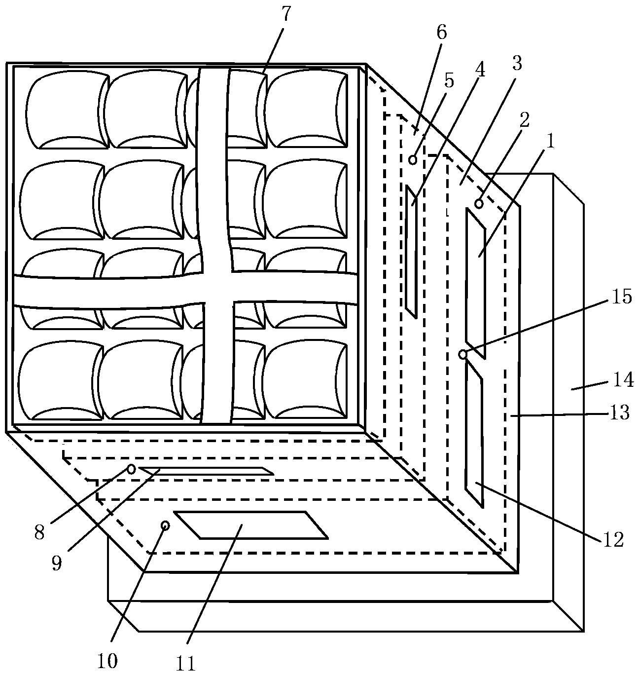
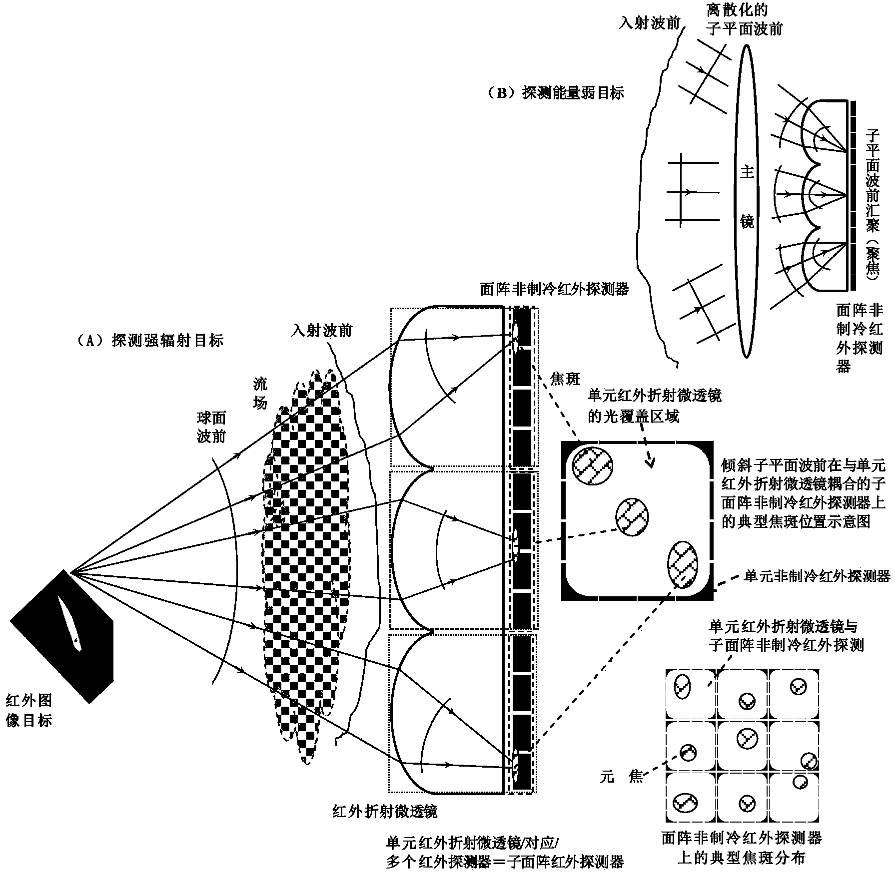
[0023] like figure 1 As shown, the infrared image and wavefront dual-mode integrated imaging detection chip of the present invention includes: a ceramic shell 13, a metal support and a heat sink 14, a drive control and preprocessing module 3, an area array uncooled infrared detector 6, and an area array Infrared refractive microlenses 7.

[0024] The drive control and preprocessing module 3 , the ...


PUM


Abstract

The invention discloses an infrared image and wave front dual mode integrated imaging detection chip which comprises a ceramic shell, a metal support, a heat dissipation board, a drive control and preprocessing module, an area array non-refrigeration infrared detector and an area array infrared refraction micro lens. The drive control and preprocessing module, the area array non-refrigeration infrared detector and the area array infrared refraction micro lens are coaxially and sequentially arranged in the ceramic shell. The rear portion of the ceramic shell is arranged on the top of the metal support and the top of the heat dissipation board. The drive control and preprocessing module is arranged at the joint of the rear portion of the ceramic shell, the metal support and the heat dissipation board. The area array non-refrigeration infrared detector is arranged on the top of the drive control and preprocessing module, and the area array infrared refraction micro lens is arranged on the top of the area array non-refrigeration infrared detector, wherein the light incident plane of the area array infrared refraction micro lens is exposed through an open hole in the face portion of the ceramic shell, and the area array infrared refraction micro lens comprises M*N unit micro lenses. The infrared image wave front dual mode integrated imaging detection chip is compared in structure, convenient to use, capable of being easily compatible or coupled with a conventional infrared optical system and good in adaptability of a target and the environment.

Description

technical field [0001] The invention belongs to the technical field of infrared imaging detection, and more particularly relates to an infrared image and wavefront dual-mode integrated imaging detection chip. Background technique [0002] Generally speaking, light waves emitted by natural and artificial light sources constitute the background electromagnetic radiation environment in which the target depends. The atmospheric flow field often produces unstable or non-equilibrium changes in density, temperature, pressure and composition. The special physical and chemical behaviors of gas molecules, such as ionization effect, also promote the instability or even random change of their dielectric properties, so that the optical refractive index of the flow field presents complex time-varying or space-varying characteristics, thus affecting the target light waves in the atmosphere. The transmission of different levels of interference or even suppression. The outgoing beam, which...

Claims


Application Information

Patent Timeline
Patent Type & Authority Applications(China)
IPC IPC(8): G01J5/10G01J9/00
Inventor 张新宇佟庆康胜武罗俊桑红石谢长生
Owner HUAZHONG UNIV OF SCI & TECH
Why Eureka
Try Eureka