Selective absorption filtering structure

A technology of selective absorption and medium, applied in optics, optical components, instruments, etc., can solve the problems of degradation of absorption efficiency, complex preparation process, sensitivity to the polarization state of incident light, etc., to achieve the effect of easy implementation and simple preparation process

Active Publication Date: 2014-01-15
SUZHOU UNIV +1
View PDF4 Cites 34 Cited by
  • Summary
  • Abstract
  • Description
  • Claims
  • Application Information

AI Technical Summary

Problems solved by technology

The problem is that it is easy to fade, and the ink contains harmful substances such as aromatic hydrocarbons, heavy metals, benzene, and ketones, which are very harmful to operators and the environment during the production and printing of inks
[0004] The problems existing in the existing technology are: (1) Most of the designed structures work at a single wavelength, and the absorption efficiency at other wavelengths drops significantly, but broadband absorption is more valuable for stealth, thermal emission and energy conversion; ( 2) It is sensitive to the polarization state of the incident light, and the absorption efficiency degrades seriously in a wide range of incident angles; (3) The current selective absorber is mainly aimed at the microwave and terahertz bands, and is mainly used in detection, which limits its use in other field application
Although these two structures achieve selective absorption in a wide band and a wide range of incident angles, the preparation process is complicated.

Method used


Image

  • Selective absorption filtering structure
  • Selective absorption filtering structure
  • Selective absorption filtering structure

Examples


Embodiment 1

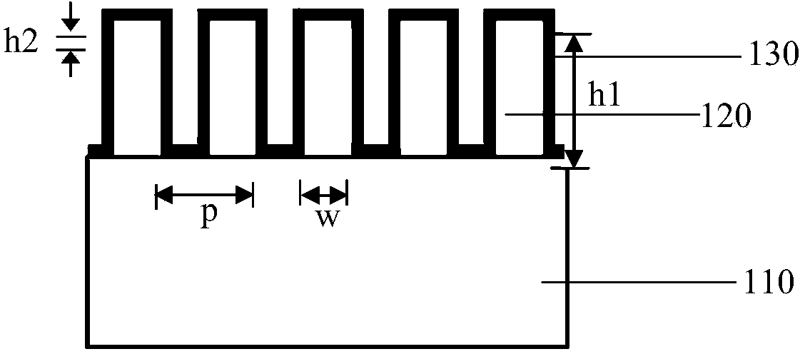
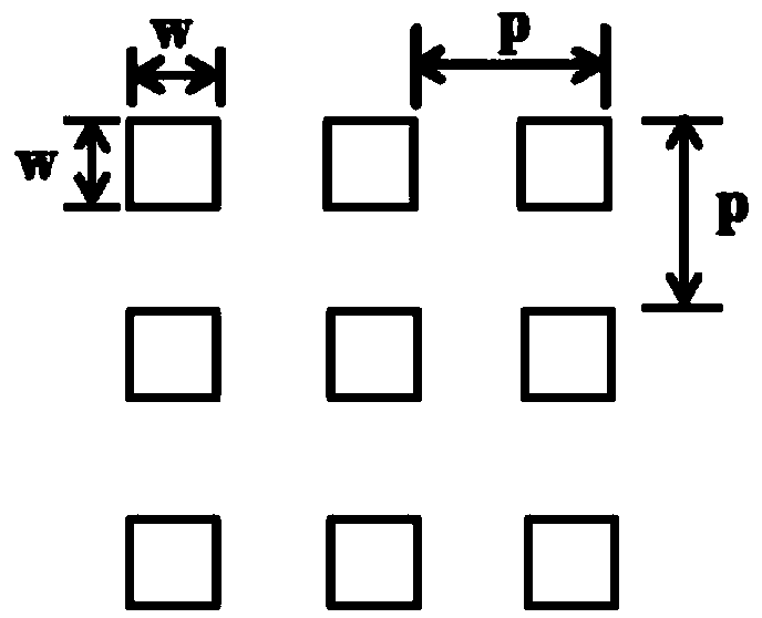
[0037] In this embodiment, nickel is used as the metal layer, and the dielectric constant of nickel is as follows: Figure 11 As shown, wherein the solid line represents the real part in the dielectric constant, and the dotted line represents the imaginary part. It can be seen that the real part and the imaginary part of the dielectric constant of nickel meet the requirements of the present invention in the visible light range, that is, the imaginary part is greater than the real part. The absolute value of the part. see figure 1 , in this embodiment, the substrate 110 is a flexible material, specifically PET or PC. The medium micro-nano unit 120 is a nano-square column arranged in a quadrilateral, as shown in FIG. 2( a ). Metal layer 130 is nickel. Further, the period of the medium micro-nano unit is p=220nm, the duty ratio is F=0.4, and the thickness h1=100nm. Metal layer thickness h2=20nm.

[0038] The absorption characteristics and angle tolerance of selective absorpt...

Embodiment 2

[0043] In this embodiment, the material of the metal layer is changed, the metal layer 130 is chromium, and the dielectric constant of chromium is as follows Figure 12 As shown, wherein the realization represents the real part of the dielectric constant, and the dotted line represents the imaginary part. It can be seen that the real part and the imaginary part of the dielectric constant of chromium meet the requirements of the present invention in the visible light range, that is, the imaginary part is greater than the absolute value of the real part . Please continue to see figure 1 , in this embodiment, the substrate 110 is a flexible material, specifically PET or PC. The medium micro-nano unit 120 is a nano-square column arranged in a quadrilateral, as shown in FIG. 2( a ). Further, the period of the medium micro-nano unit is p=220nm, the duty ratio is F=0.4, and the thickness h1=100nm. Metal layer thickness h2=20nm.

[0044] The absorption characteristics and angle to...

Embodiment 3

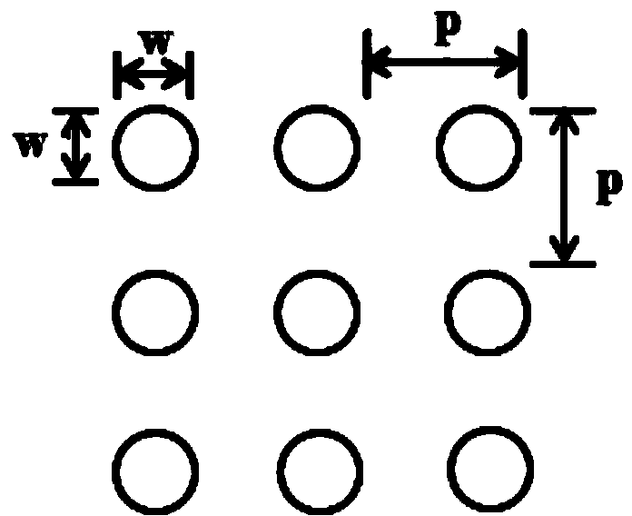
[0049] In this embodiment, by changing the shape of the medium micro-nano unit, the influence of the shape of the medium micro-nano unit on the effect of the selective filter structure of the present invention is studied. As shown in FIG. 2( b ), the substrate 110 is a flexible material, specifically PET or PC. The dielectric micro-nano unit 120 is nano-circular pillars arranged in a quadrangular shape, and the metal layer 130 is chromium. Further, the period of the medium micro-nano unit is p=220nm, the duty ratio is F=0.4, and the thickness h1=100nm. Metal layer thickness h2=20nm.

[0050] The absorption characteristics and angle tolerance of selective absorption filter structures are analyzed by rigorous coupled wave theory (RCWA). TM and TE polarized light is incident from the top of the structure at angles ranging from 0° to 45°.

[0051] Figure 7 The relationship diagram of the absorption spectrum of the TM polarized light of the selective absorption filter structur...


PUM

PropertyMeasurementUnit
thicknessaaaaaaaaaa
thicknessaaaaaaaaaa

Abstract

A selective absorption filtering structure comprises a substrate, a dielectric micro-nano unit located on the substrate and a metal layer located on the dielectric micro-nano unit. The metal layer totally covers the dielectric micro-nano unit, namely, the metal layer covers the ridge portion, the slot portion and the side wall of the dielectric micro-nano unit. The imaginary part of the dielectric constant of the metal layer needs to be larger than the absolute value of the real part of the dielectric constant. The filtering structure has relatively high absorption efficiency and is not sensitive to the angle and the polarization state of incident light. Meanwhile, manufacturing process is simple and easy to achieve. The structure can be applied to a solar cell to capture more energy and can provide a solution for achieving black in non-ink printing, and a traditional concept that black printing can be achieved only by means of pigments is changed.

Description

technical field [0001] The invention relates to an optical filter element, in particular to a selective absorption filter structure, which can be applied to the fields of light display, photovoltaic, solar cell, ink-free printing and the like. Background technique [0002] Selective absorption is mainly used in the fields of stealth, thermal emission, light display, photovoltaics, solar cells, and ink-free printing. For example: (1) In the field of printing, the traditional printing technology is to print images and colors on the surface of paper, plastic and other materials through inks of different colors. The existing problems are: it is easy to fade, and the ink contains harmful substances such as aromatic hydrocarbons, heavy metals, benzene, and ketones, which are very harmful to operators and the environment during the production and printing of the ink. Existing designs mainly focus on designing micro-nanostructures to achieve magenta, cyan, and yellow, and there is ...

Claims


Application Information

Patent Timeline
Patent Type & Authority Applications(China)
IPC IPC(8): G02B5/22
Inventor 周云陈林森申溯叶燕
Owner SUZHOU UNIV
Why Eureka
Try Eureka