Method for testing light transmittance performance of optical waveguide

An optical waveguide and performance technology, which is used in the field of testing the optical performance of optical waveguides based on scanning near-field optical microscopes, can solve problems such as complex experimental skills, surface damage of waveguides, and optical waveguide ratios, and achieves simple structure, Small size and easy operation

Inactive Publication Date: 2014-01-22
INST OF SEMICONDUCTORS - CHINESE ACAD OF SCI
View PDF5 Cites 11 Cited by
  • Summary
  • Abstract
  • Description
  • Claims
  • Application Information

AI Technical Summary

Problems solved by technology

The sliding prism method needs to repeatedly slide the prism on the surface of the waveguide, which requires very complicated experimental skills and will cause damage to the surface of the waveguide
The prism coupling method requires a relatively long optical waveguide

Method used


Image

  • Method for testing light transmittance performance of optical waveguide
  • Method for testing light transmittance performance of optical waveguide
  • Method for testing light transmittance performance of optical waveguide

Examples


Embodiment

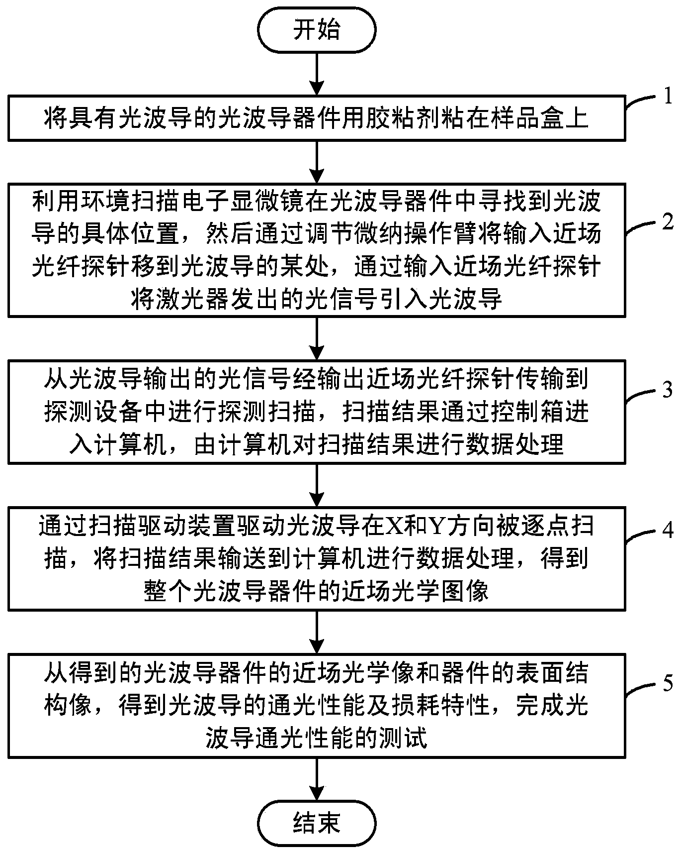
[0037] The method for testing the light transmission performance of an optical waveguide based on the scanning near-field optical microscope proposed by the present invention can test the light transmission performance of various optical waveguides. The Mach-Zehnder modulator is used as an example to illustrate in detail below.

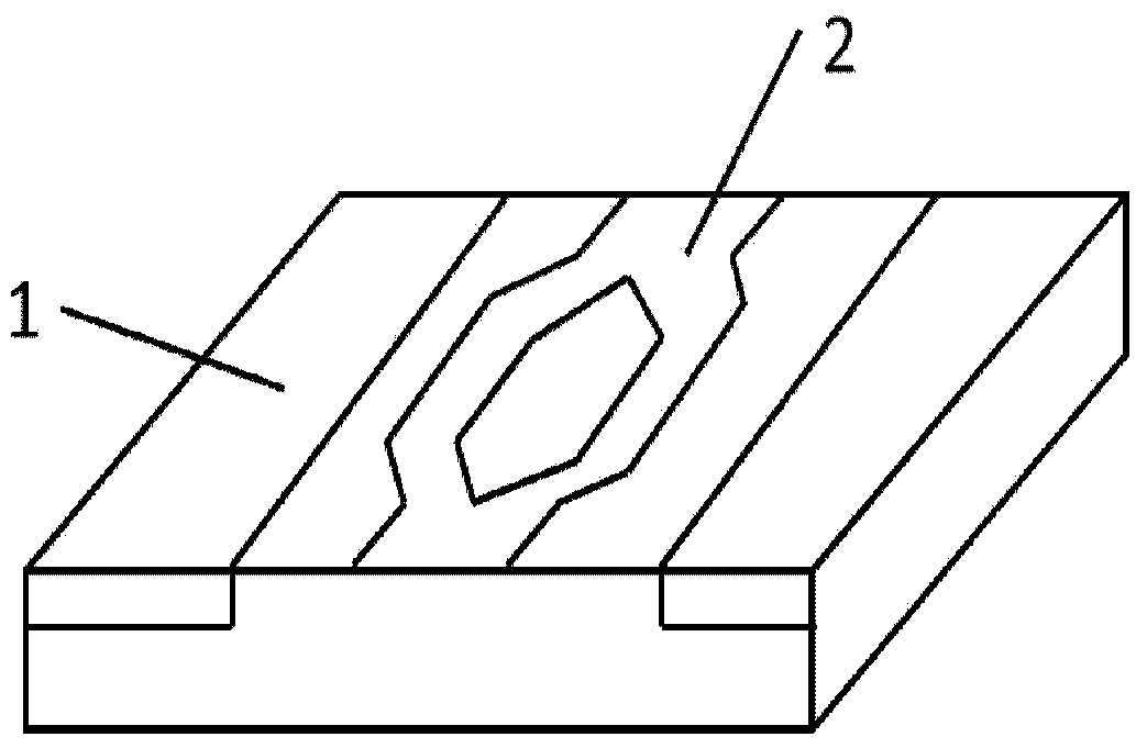
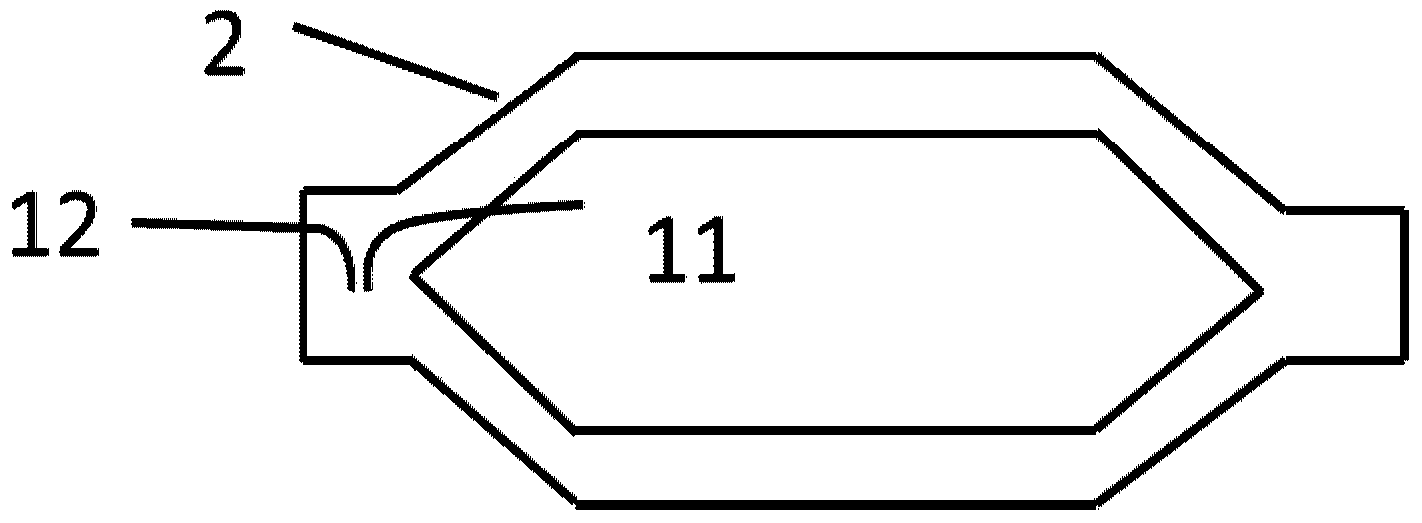
[0038] The structure of the Mach-Zendr modulator is as follows figure 2 As shown, it includes an insulating layer 1 and an optical waveguide 2, and the middle of the insulating layer 1 is an optical waveguide 2. This embodiment is to test the light transmission characteristics of the optical waveguide 2 in the Mach-Zehnder modulator, specifically including:

[0039] Firstly, dip a small amount of glue from the white latex glue bottle with tweezers, and apply it to the back of the prepared Mach-Zender modulator chip, and fix it on the sample box. The length and width of the glue coating should be smaller than the size of the Mach-Zehnder modulator chi...


PUM


Abstract

The invention discloses a method for testing the light transmittance performance of an optical waveguide on the basis of a scanning near-field optical microscope. The method is realized on the basis of a testing system which comprises a laser device, an optical waveguide device provided with the optical waveguide, a scanning and driving device, an input near-field optical fiber probe, an output near-field optical fiber probe, a signal generator, a phase-locking amplifier, a micro nano operation arm, detection equipment, a control box and a computer. The method comprises the steps as follows: firstly, the manufactured waveguide device is bonded on a sample box with an adhesive; then the accurate position of the optical waveguide is found through an electron microscope, the near-field optical fiber probes are moved to a certain position of the optical waveguide through the micro nano operation arm, and a light signal is introduced by the input near-field optical fiber probe; an output light signal is transmitted into detection equipment through the output near-field optical fiber probe; the optical waveguide is driven to be scanned point by point in the X-direction and the Y-direction through a scanning platform, so that a near-field optical image of the whole optical waveguide is obtained; and testing of an optical waveguide chip is completed. According to the method, the light transmittance performance of the optical waveguide device can be tested accurately.

Description

technical field [0001] The invention relates to the technical field of optical waveguide device testing, in particular to a method for testing the optical performance of an optical waveguide based on a scanning near-field optical microscope. Background technique [0002] Since the appearance of the optical microscope, people have been making unremitting efforts to improve the resolution of the microscope. Since the 18th century, the resolution of optical microscopes has not improved substantially, mainly due to the existence of a resolution limit determined by diffraction effects. Subsequently, scanning electron microscopes, scanning tunneling microscopes, etc. were proposed. Although the resolution of these microscopes has been amazingly improved, they have some fundamental weaknesses. For example, they have high requirements on the sample, and also have high requirements on the environment of the sample, so that the use of this type of microscope is limited. Therefore, p...

Claims


Application Information

Patent Timeline
Patent Type & Authority Applications(China)
IPC IPC(8): G01M11/02
Inventor 杨惠霞谢亮王瑞
Owner INST OF SEMICONDUCTORS - CHINESE ACAD OF SCI
Why Eureka
Try Eureka